Backlight type photoelectric anode and preparing method and application thereof
A photoelectric anode and electrode technology, applied in the direction of electrodes, electrolysis process, electrolysis components, etc., can solve the problems of unsuitable industrial production, cumbersome steps, expensive raw materials, etc.
- Summary
- Abstract
- Description
- Claims
- Application Information
AI Technical Summary
Problems solved by technology
Method used
Image
Examples
Embodiment 1
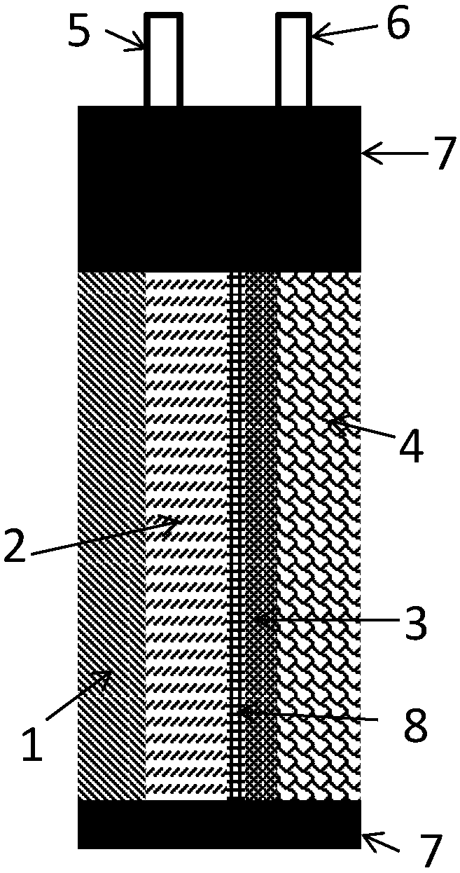
[0082] This embodiment provides a method for preparing a back-illuminated photoanode, the specific method of which is:
[0083] (1) Preparation of n by thermal diffusion on p-type silicon + emitter, then the n + The emitter is plated with 70nm-80nm silicon nitride as an anti-reflection layer, and a silver electrode is made on the anti-reflection layer by a screen printing process to obtain a silicon-based solar cell with a pn junction and an exposed anode, which is used as the substrate 2. TiO was prepared on one side of the substrate 2 by atomic layer deposition x Protective film 8, prepare the nickel film that thickness is 100nm with the method for thermal evaporation on protective film 8 again, lead out second electrode 6 on described nickel film and package with sealing material 7, described second electrode 6 uses conductive The slurry is connected to the transition metal film;
[0084] (1') Cover transparent conductive glass 1 on one side of substrate 2, and described...
Embodiment 2
[0092] This embodiment provides a method for preparing a back-illuminated photoanode, the specific method of which is:
[0093] (1) Adopting a commercial copper indium gallium selenide (CIGS) solar cell with a pn junction and an exposed anode as the substrate 2, preparing a nickel-iron alloy film with a thickness of 200 nm by thermal evaporation on one side of the substrate 2, The second electrode 6 is drawn out on the nickel-iron alloy film and packaged with a sealing material 7, and the second electrode 6 is connected to the transition metal film with solder;
[0094] (1') cover transparent conductive glass 1 on one side of substrate 2, described transparent conductive glass 1 and nickel-iron alloy film are respectively positioned at the both sides of described substrate 2, the method of covering transparent conductive glass 1 is welding;
[0095] (2) n from the substrate + One end of the emitter leads to the first electrode, and the first electrode is made of indium galliu...
Embodiment 3
[0101] This embodiment provides a method for preparing a back-illuminated photoanode. For the specific method, refer to Example 1. The difference is:
[0102] In step (1), according to required TiO x The thickness of protective film 8 is adaptively adjusted to the operating conditions of atomic layer deposition, and the method preparation thickness with electron beam evaporation is the nickel film of 10nm, in step (3), according to the thickness of required nickel-iron double metal hydroxide to Adaptive adjustments were made to the electrodeposition operating conditions.
[0103] Refer to Example 1 for the structure of the back-illuminated photoanode prepared in this example. The difference is that the activated transition metal film 3 of the back-illuminated photoanode obtained in this embodiment is an activated nickel film with a thickness of 10 nm, and the transition metal catalyst layer 4 is a nickel-iron double metal hydroxide with a thickness of 10 nm. 2μm, protective ...
PUM
| Property | Measurement | Unit |
|---|---|---|
| thickness | aaaaa | aaaaa |
| thickness | aaaaa | aaaaa |
| thickness | aaaaa | aaaaa |
Abstract
Description
Claims
Application Information
