System for generating broadband radio frequency signal

A radio frequency signal and generation system technology, applied in the field of communications, can solve the problems of inability to directly generate radio frequency signals, inability to generate radio frequency signals, and low flexibility in generating signals, achieving simple and flexible implementation methods, overcoming clock rate mismatch, Bandwidth effect

Active Publication Date: 2018-07-20
中国人民解放军火箭军工程大学
View PDF10 Cites 1 Cited by
  • Summary
  • Abstract
  • Description
  • Claims
  • Application Information

AI Technical Summary

Problems solved by technology

[0002] For the development of broadband signal sources, Rao Ruinan implemented a 0.1-5GHz comb spectrum generator by building an analog circuit and using step recovery diodes. Although this type of method can generate signals with a larger bandwidth, the signal pattern that can be generated Insufficient richness; In view of the low flexibility of analog signal generation, Yan Guanghua, Liu Yujun and others used DDS technology to propose a method of using FPGA to generate baseband digital signal data to generate signals; Qing Hao further implemented this method, using Xilinx Virtex4 FPGA and AD9957 chip as the core, designed a signal source that can generate a maximum hop speed of 200Khops/s in the 40-240MHz bandwidth range, but it can only generate frequency hopping signals, which limits the application range of the device; Dong Keqiang designed with AD9953 as the core 0-150MHz broadband signal source, but it can only generate baseband ...

Method used


Image

  • System for generating broadband radio frequency signal
  • System for generating broadband radio frequency signal
  • System for generating broadband radio frequency signal

Examples


Embodiment 1

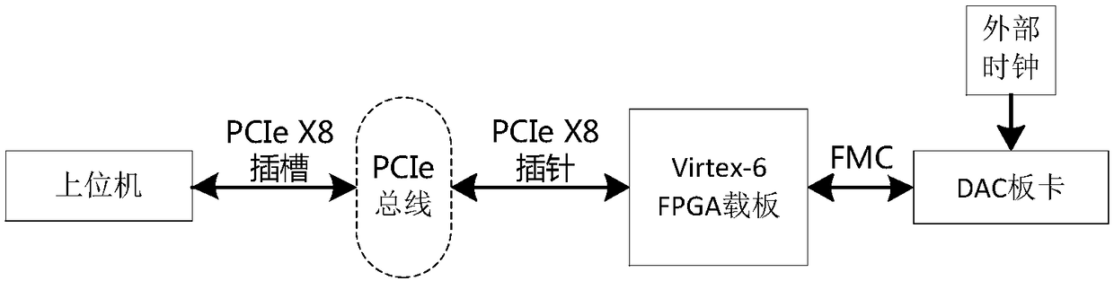
[0037] This embodiment provides a broadband radio frequency signal generation system, such as figure 1 , including the host computer, PCIe bus, FPGA main board, and DAC board. The host computer is used to generate digital signal signals and transmit analog signals to the FPGA main board through the PCIe bus. The FPGA main board transmits digital signals to the DAC board through the control logic unit;

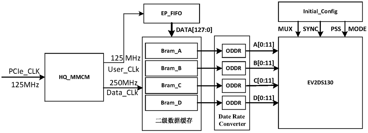
[0038] like image 3 , the control logic unit includes: a clock management module, a data cache module, a secondary data cache module, a data rate conversion module, and an initialization configuration logic module;

[0039] The clock management module is used to receive the 125MHz clock signal from the PCIe bus, divide and process the 125MHz clock signal into one 125MHz clock signal and one 250MHz clock signal, transmit one 125MHz clock signal to the data cache module, and transfer one A 250MHz clock signal is transmitted to the secondary data cache module;

[0040]Designed ...

Embodiment 2

[0048] The present embodiment provides the concrete structure of upper computer on the basis of embodiment 1, comprises board card control module, parameter input and data generation module, waveform chart drawing module; Described board card control module is used to provide to user interface to control The status of the DAC board card and the RF signal sampling data generated by the user are sent to the signal board to correctly generate the signal. The parameter input and data generation module is used for this module to provide the user with a visual interface to select the interference signal style that needs to be generated and Corresponding parameters, and call MATLAB according to the input parameters to complete the generation of signal sampling data files; the waveform diagram drawing module is used to draw the time domain waveform diagram and spectrum diagram of the interference signal designed by the user, so that the user can observe designed interference signal.

...

Embodiment 3

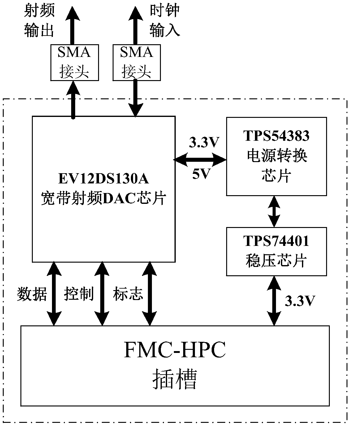
[0061] This embodiment provides the specific structure of the DAC board on the basis of Embodiment 1, such as figure 2 , DAC board includes DAC chip, power conversion chip, voltage regulator chip and FMC-HPC interface, FMC-HPC interface is used to convert 3.3V power supply to 5V voltage, 5V voltage passes through voltage regulator chip, power conversion chip and DAC chip electrical connection;

[0062] The external clock signal is input into the DAC chip through the SMA connector, and the DAC video signal is output through the SMA connector.

[0063] The DAC board is based on the EV12DS130A chip, which can directly have an analog output bandwidth of 7GHz without relying on the up-converter module. It also has 12-bit resolution and four different operating modes of RTZ, NRZ, NRTZ, and RF to choose from. Its clock resolution Reaching 0.0625Hz, the operation of the board is simple and flexible, and there are reserved configuration and status observation bit ports. In order to ...


PUM


Abstract

The invention discloses a system for generating a broadband radio frequency signal, comprising a host computer, a PCIe bus, an FPGA main board and a DAC board, wherein the host computer is configuredto generate a digital signal and transmit an analog signal to the FPGA main board through the PCIe bus, the FPGA main board is configured to transmit the digital signal to the DAC board through a control logic unit, and the control logic unit includes a clock management module, a data cache module, a secondary data cache module, a data rate conversion module and an initialization configuration logic module. The invention has the advantages that the system is large in bandwidth of the generated radio frequency signal, high in precision, high in hardware design integration and less in device usage, the data transmission logic overcomes the shortage of clock rate mismatch of the FPGA and DAC, the host computer software supports rich signal patterns, the implementation manner is simple and flexible, and various types of wideband radio frequency signals can be generated in a relatively simple manner under a small volume to meet the needs of various application scenarios.

Description

technical field [0001] The invention belongs to the technical field of communication, and in particular relates to a broadband radio frequency signal generating system. Background technique [0002] For the development of broadband signal sources, Rao Ruinan implemented a 0.1-5GHz comb spectrum generator by building an analog circuit and using step recovery diodes. Although this type of method can generate signals with a larger bandwidth, the signal pattern that can be generated Insufficient richness; In view of the low flexibility of analog signal generation, Yan Guanghua, Liu Yujun and others used DDS technology to propose a method of using FPGA to generate baseband digital signal data to generate signals; Qing Hao further implemented this method, using Xilinx Virtex4 FPGA and AD9957 chip as the core, designed a signal source that can generate a maximum hop speed of 200Khops / s in the 40-240MHz bandwidth range, but it can only generate frequency hopping signals, which limit...

Claims


Application Information

Patent Timeline
IPC IPC(8): H03L7/18G06F17/50G06F13/40G06F13/42
CPCG06F13/4068G06F13/4221G06F30/331H03L7/18
Inventor 杨剑张月刘瑞麒鲍庆龙余志勇卢建
Owner 中国人民解放军火箭军工程大学
Why Eureka
Try Eureka