Supercharge Your Innovation With Domain-Expert AI Agents!

A kind of manufacturing method of multi-layer Teflon circuit board

A production method and circuit board technology, applied in the field of circuit board manufacturing, can solve the problems of warping, low melting temperature, and hollow glass fiber, improve quality and yield, optimize the entire process, and solve the problem of explosion and delamination. Effect

Active Publication Date: 2020-04-14
SHENZHEN SUNTAK MULTILAYER PCB
View PDF7 Cites 0 Cited by
  • Summary
  • Abstract
  • Description
  • Claims
  • Application Information

AI Technical Summary

Problems solved by technology

UHF materials are usually made of mixed pressure of Teflon and glass fiber. Due to the asymmetry of the structure of the two materials and the difference in physical properties of the materials, the force between Teflon and glass fiber is very weak, resulting in Problems such as delamination and warping of the board often occur during processing and placement of finished products
At the same time, it will also lead to problems such as the glass fiber is not suitable to be cut to form copper nodules, or the glass fiber is broken to form a hollow.
[0003] At the same time, the melting temperature (Tm) of Teflon material is low, the material is relatively soft, and it is easy to melt and stick to the hole wall when drilling, leaving a large amount of filamentous debris on the hole wall, and because of its stable chemical properties (acid-resistant Alkali), making the resin residue difficult to remove, easy to produce large nail heads

Method used


Image

  • A kind of manufacturing method of multi-layer Teflon circuit board
  • A kind of manufacturing method of multi-layer Teflon circuit board
  • A kind of manufacturing method of multi-layer Teflon circuit board

Examples


Embodiment

[0033] The invention provides a kind of manufacture method of multi-layer Teflon circuit board, comprises the following steps:

[0034] S1. Cut the Teflon substrate according to the required size to obtain the cutting board, bake the cutting board, the baking temperature is 150°C, and the baking time is 4 hours;

[0035] S2, roughen the surface of the cutting board, the roughening method is a roughening method other than mechanical grinding;

[0036] S3, making the inner layer circuit on the cutting board to obtain the inner layer board;

[0037] S4. Browning the copper surface on the inner layer board to obtain a browning board, wherein the browning rate is 3.0m / min; baking the browning board, the baking temperature is 150°C, and the baking time is 120min;

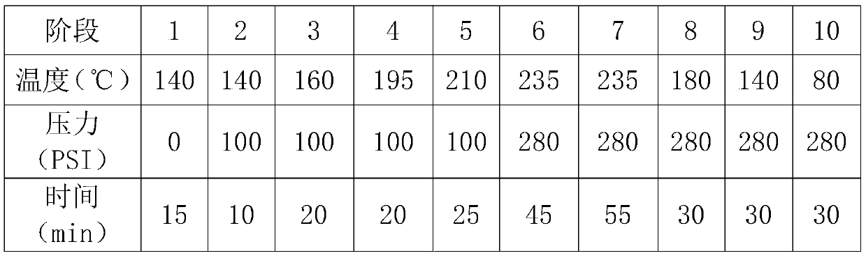
[0038] S5. Stack and press each board to make a multi-layer board; multi-stage pressing includes ten stages, and the specific method is as follows: the first stage pressing temperature is 140°C, pressing pressure is 0psi...


PUM


Abstract

The invention relates to the circuit board manufacturing field and specifically relates to a multilayer teflon circuit board manufacturing method. The method focuses on control of pressing process through a multistage pressing method, optimizes overall process flow and solves the problems of board delamination and warping and the like due to different physical properties of Teflon and glass fibermaterials. By placing a pad plate on the bottom portion of a multilayer board and covering a phenolic resin plate on the surface thereof, and then, through hole drilling and slotting process, powdersof the phenolic resin plate on the surface are allowed to be mixed with teflon filamentous residues, thereby reducing viscosity of the teflon filamentous residues, and preventing the phenomenon of generation of a big nail head; through a plasma cleaning process, residues stuck to the wall of each hole during drilling is removed; and through the plasma cleaning process, resin residues are allowed to be cleared easily, thereby improving overall quality and rate of finished products of the multilayer teflon circuit board.

Description

technical field [0001] The invention relates to the field of circuit board manufacturing, in particular to a method for manufacturing a multilayer Teflon circuit board. Background technique [0002] Under the trend of high-frequency communication, high-speed transmission and communication confidentiality, it is required to achieve low loss and low delay of transmission signals, and high-frequency plates with low Dk, low Df, and high temperature resistance must be selected; there are many high-frequency substrates that meet these requirements , such as polyphenylene ether, cyanate, polybutadiene, etc., among which polytetrafluoroethylene (Teflon, PTFE) is more commonly used. Based on the requirements of UHF, Teflon, an UHF material with high and low temperature resistance and aging resistance, must be selected. UHF materials are usually made of mixed pressure of Teflon and glass fiber. Due to the asymmetry of the structure of the two materials and the difference in physical ...

Claims


Application Information

Patent Timeline
Patent Type & Authority Patents(China)
IPC IPC(8): H05K3/00H05K3/46
CPCH05K3/0011H05K3/0055H05K3/4626H05K2203/02
Inventor 孙保玉彭卫红宋建远宋清
Owner SHENZHEN SUNTAK MULTILAYER PCB
Features
  • R&D
  • Intellectual Property
  • Life Sciences
  • Materials
  • Tech Scout
  • Unparalleled Data Quality
  • Higher Quality Content
  • 60% Fewer Hallucinations
Learn More