Electromagnetic wave absorber based on refractory material

A refractory material and absorber technology, applied in instruments, optical components, optics, etc., can solve the problems of strong ohmic loss and thermal effect, inability to achieve broadband light absorption, poor structural stability of precious metal micro-nano materials, etc. Effect

Inactive Publication Date: 2018-07-27
JIANGXI NORMAL UNIV
View PDF9 Cites 9 Cited by
  • Summary
  • Abstract
  • Description
  • Claims
  • Application Information

AI Technical Summary

Problems solved by technology

However, in these three-layer perfect electromagnetic wave absorber systems, they can only absorb electromagnetic waves with a narrow band and a single resonant wavelength, and cannot achieve broadband light absorption in the ultraviolet, visible, and near-infrared bands, thus limiting the above-mentioned perfect electromagnetic wave absorbers. Wide application in technical fields such as infrared filters and photodetectors
[0006] In addition, these electromagnetic wave perfect absorber systems are all based on noble metal materials and their micro-nano structures. The coupling of electromagnetic waves is realized through the free electron oscillation modes of these noble metal materials. These free electron oscillations will inevitably lead to strong ohmic losses and thermal effects, resulting in noble metal micro The structural stability of nanomaterials is relatively poor, which makes the use range of the above-mentioned perfect electromagnetic wave absorber relatively small, which further limits the application prospects of this type of absorber under high-intensity electromagnetic wave irradiation

Method used


Image

  • Electromagnetic wave absorber based on refractory material
  • Electromagnetic wave absorber based on refractory material
  • Electromagnetic wave absorber based on refractory material

Examples


Embodiment 1

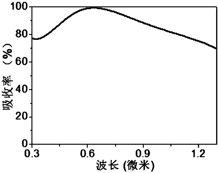
[0047] figure 2 Shown is a light absorption diagram of an embodiment of the electromagnetic wave absorber based on refractory materials of the present invention. The particle structure layer only contains an array of tungsten cylindrical particles of one size. The substrate is a silicon wafer, and the thickness of the tungsten film is 100 nanometers. The material of the dielectric film layer is aluminum oxide with a thickness of 40 nanometers. The particle diameter in the tungsten cylindrical particle array is 100 nanometers and the thickness is 40 nanometers. The particle array is a square array with a lattice constant of 150 nanometers.

[0048] From figure 2 It can be determined from the spectrogram shown that the absorption rate at a wavelength of 0.634 microns reaches a maximum of 99.4%. In the spectral range from 0.469 microns to 0.867 microns, a wide-band perfect absorption spectrum with an absorption rate of over 90% is produced, that is, the perfect absorption bandw...

Embodiment 2

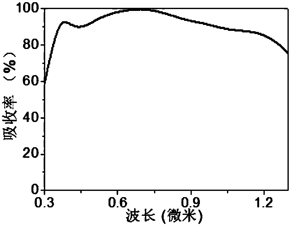
[0050] image 3 Shown is the light absorption diagram of the second embodiment of the electromagnetic wave absorber based on refractory materials of the present invention. The particle structure layer only contains an array of vanadium cylindrical particles of one size. The substrate is a silicon wafer, and the thickness of the vanadium film is 100 nanometers. The material of the dielectric film layer is aluminum oxide with a thickness of 40 nanometers. The particle diameter in the vanadium cylinder particle array is 100 nanometers and the thickness is 40 nanometers. The particle array is a square array with a lattice constant of 150 nanometers.

[0051] From image 3 It can be determined from the spectrogram shown that the absorption rate at the wavelength of 0.684 microns reaches the maximum value of 99.7%. In the spectral range from 0.360 microns to 1.008 microns, a wide-band perfect absorption spectrum with an absorption rate of over 90% is produced, that is, the perfect a...

Embodiment 3

[0053] Figure 4 Shown are the three light absorption diagrams of the embodiment of the electromagnetic wave absorber based on refractory materials of the present invention. The particle structure layer only contains an array of tantalum cylinder particles of one size. The substrate is a quartz plate, and the thickness of the tantalum film is 100 nanometers. The material of the dielectric film layer is aluminum oxide with a thickness of 40 nanometers. The diameter of the particles in the tantalum cylinder particle array is 100 nanometers and the thickness is 40 nanometers. The particle array is a square array with a lattice constant of 150 nanometers. The absorption rate at a wavelength of 0.616 microns reaches a maximum of 98.8%.

[0054] From Figure 4 It can be determined from the spectrogram shown that a wide-band perfect absorption spectrum with an absorption rate of over 90% is generated in the spectral range from 0.461 microns to 0.951 microns, that is, the perfect abso...


PUM

PropertyMeasurementUnit
thicknessaaaaaaaaaa
melting pointaaaaaaaaaa

Abstract

The invention discloses an electromagnetic wave absorber based on a refractory material. The electromagnetic wave absorber comprises a protective film layer, a dielectric film layer and a particle structure layer, wherein the protective film layer is arranged on the lower surface of the dielectric film layer, the particle structure layer is arranged on the upper surface of the dielectric film layer, the protective film layer is made of the refractory material, and the particle structure layer is composed of arrays in which particles of the refractory material are periodically arranged. By means of the electromagnetic wave absorber based on the refractory material, by introducing the refractory material and using the material characteristics of the refractory material itself, the material then forms electromagnetic resonance with incident electromagnetic waves, and high electromagnetic waves are formed to be absorbed; through the three-layer structure system of the protection layer, thedielectric film layer and the particle structure layer, electromagnetic resonance characteristics of the refractory material at the ultraviolet-visible-near-infrared bands are applied, and the spectral absorption of the broadband is achieved.

Description

Technical field [0001] The invention relates to the technical fields of optoelectronic functional materials and devices and photonics, in particular to an electromagnetic wave absorber based on refractory materials. Background technique [0002] Plasmonics usually refers to the collective oscillation caused by the free electrons on the surface of the metal structure under the irradiation of external electromagnetic waves, which forms a local electromagnetic field enhancement effect on the metal surface. Metamaterials refer to artificially designed composite materials with periodic structures. The concept of perfect absorber was first proposed in 2008 ("Physical Review Letters", Vol. 100, p. 207402), and it is an electromagnetic resonance absorber based on metamaterials. [0003] A typical metamaterial perfect absorber has a three-layer structure: the top layer is a two-dimensional periodic array of metal microstructure units with single or multiple electromagnetic response modes, ...

Claims


Application Information

Patent Timeline
Patent Type & Authority Applications(China)
IPC IPC(8): G02B5/00
CPCG02B5/003G02B5/008
Inventor 刘正奇刘桂强陈齐奇唐鹏刘晓山
Owner JIANGXI NORMAL UNIV
Why Eureka
Try Eureka