

Method for judging Fermi energy level pinning effect of electronic device
A Fermi level, pinning effect technology, applied in the direction of electrical components, semiconductor devices, semiconductor/solid-state device manufacturing, etc., to achieve the effect of simple process and easy operation
- Summary
- Abstract
- Description
- Claims
- Application Information
AI Technical Summary
Problems solved by technology
Method used
Image

Examples
specific Embodiment approach 1
[0023] A method for judging the pinning effect at the Fermi level of an electronic device, comprising the following steps:
[0024] 1. Determine the thickness of the device chip;
[0025] 2. Use SRIM or Geant4 software to calculate the number of vacancies generated by a single irradiated particle in the chip material, and determine the type and energy of the irradiated particle:
[0026] The type of irradiated particles is required to be particles with atomic number not less than 6;
[0027] The energy of irradiated particles is determined by the energy that the number of vacancies produced by a single irradiated particle is greater than 1000;
[0028] In the simulation process, the device chip needs to input the chemical composition elements and the thickness of each layer of the material used, and input the type and energy of the irradiated particles. When the number of vacancies produced by a single particle of the irradiated particle is greater than 1000, the particle me...
specific Embodiment approach 2
[0034] In step 4 of this embodiment, the forward bias voltage U of the DLTS equipment test parameter during the deep-level transient spectrum test is P , reverse bias voltage U R It is determined by the C-V curve; the C-V curve is the curve of capacitance changing with the applied voltage.
[0035] DLTS equipment test parameters test period t during deep level transient spectrum test w , pulse width t p Determined by a constant temperature static test to ensure that the defect is completely filled.
[0036] The scanning temperature range T of the DLTS device test parameters during the deep-level transient spectrum test is determined by the positions of different types of defect levels in the device substrate or base material.
[0037] Other steps and parameters are the same as those in the first embodiment.
Embodiment
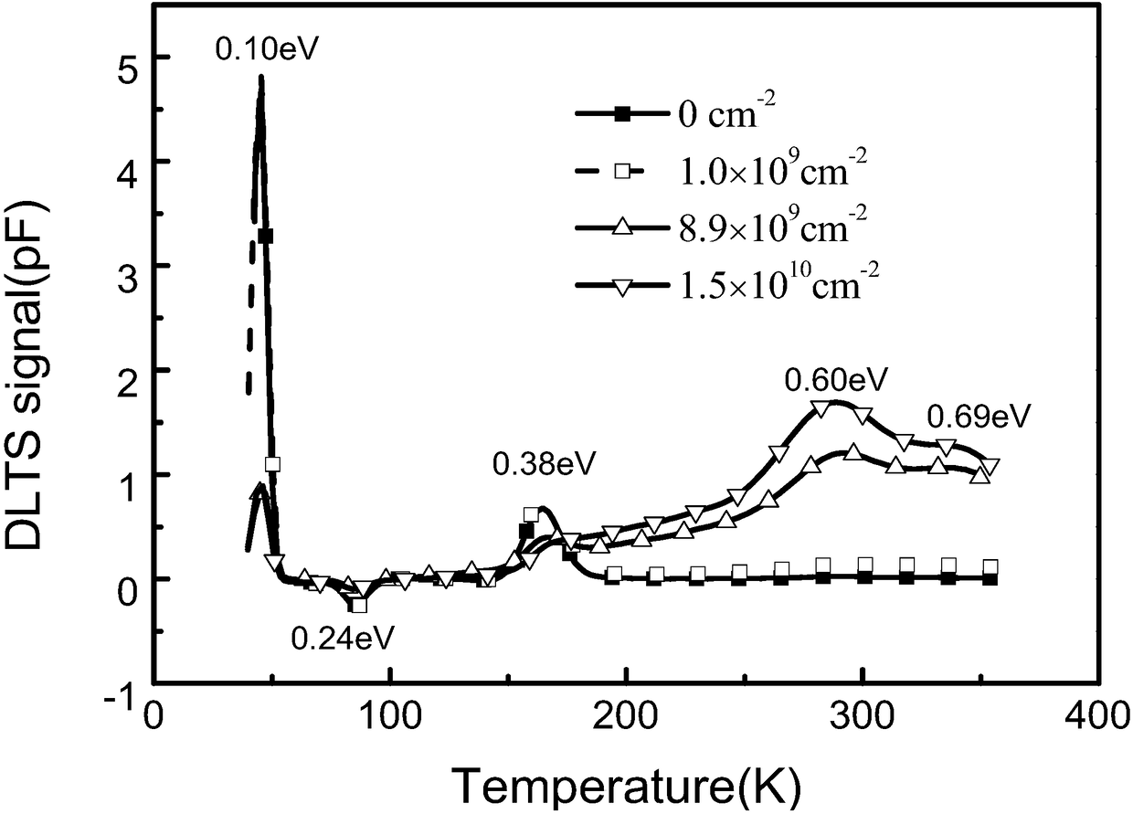
[0039] According to the DLTS results, under normal circumstances, as the irradiation fluence increases, the defect concentration increases, and the DLTS signal peak intensity should also increase accordingly. However, if the irradiation fluence increases and the local defect concentration is too high, the Fermi level is pinned to the deep energy level, so that the shallow energy level cannot be filled by the DLTS signal, and the signal intensity of the shallow energy level DLTS peak decreases. If the phenomenon is abnormal, it proves that the pinning effect of the Fermi level has occurred.
[0040] Carry out experiment according to specific embodiment two, the result is as follows figure 1 or figure 2 shown.
[0041] figure 1 The DLTS results of SiC Schottky diodes irradiated by 40 MeV Si ions are shown. Where beforeirradiation represents the corresponding curve before irradiation.
[0042] figure 1 In the figure, with the increase of the irradiation fluence, the two ki...
PUM
 Abstract
Description
Claims
Application Information