Preparation method of InGaN thin film

A thin film and substrate technology, applied in the field of InGaN thin film preparation, can solve problems such as surface roughness and phase separation

Active Publication Date: 2018-07-27
TAIYUAN UNIV OF TECH
View PDF5 Cites 17 Cited by
  • Summary
  • Abstract
  • Description
  • Claims
  • Application Information

AI Technical Summary

Problems solved by technology

[0005] The present invention aims at the problems of surface roughness, phase separation and defects caused by In segregation in existing high-quality epitaxially grown InGaN films, and provides a method for preparing InGaN films. The method grows InGaN films by digital alloy technology, that is, at high In component of In x Ga 1-x Insertion of In with low In composition in the N layer y Ga 1-y N thin layer, and remove In atoms accumulated on the growth surface by introducing a small amount of hydrogen during the growth and interruption process

Method used


Image

  • Preparation method of InGaN thin film
  • Preparation method of InGaN thin film
  • Preparation method of InGaN thin film

Examples


Embodiment 1

[0032] A method for preparing an InGaN film includes the following steps:

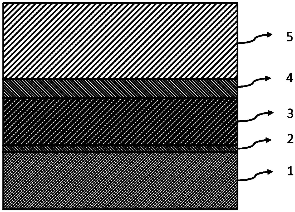
[0033] S1: Such as figure 1 As shown, a low-temperature growth GaN nucleation layer 2 is grown on a sapphire substrate 1, and the nucleation layer is annealed at a high temperature; the growth temperature of the GaN nucleation layer is 500° C., the thickness is 15 nm, and the pressure is 150 Torr. The annealing temperature is 900℃ and the time is 20min. The annealed nucleation layer transforms into an island structure with a certain grain orientation;

[0034] S2: Such as figure 1 As shown, an unintentionally doped GaN buffer layer 3 is grown on the nucleation layer 2. The growth temperature is 1150℃, the thickness is 0.2μm, and the pressure is 50 Torr;

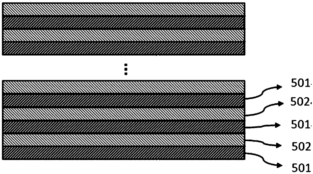
[0035] S3: Such as figure 1 As shown, a medium-high temperature GaN layer 4 is grown on the GaN buffer layer 3. The growth temperature is 750°C and the thickness is 2nm. The medium and high temperature GaN layer is beneficial to reduce the thermal stress...

Embodiment 2

[0040] A method for preparing an InGaN film includes the following steps:

[0041] S1: Such as figure 1 As shown, a low-temperature growth GaN nucleation layer 2 is grown on a silicon substrate 1, and the nucleation layer is annealed at a high temperature; the growth temperature of the GaN nucleation layer is 700° C., the thickness is 50 nm, and the pressure is 700 Torr. The annealing temperature is 1100℃, and the time is 0.5min. The annealed nucleation layer transforms into an island structure with a certain grain orientation;

[0042] S2: Such as figure 1 As shown, an unintentionally doped GaN buffer layer 3 is grown on the nucleation layer 2. The growth temperature is 1120°C, the thickness is 4μm, and the pressure is 700 Torr;

[0043] S3: Such as figure 1 As shown, a medium-high temperature GaN layer 4 is grown on the GaN buffer layer 3. The growth temperature is 1050°C and the thickness is 200 nm. The medium and high temperature GaN layer is beneficial to reduce the thermal ...

Embodiment 3

[0048] A method for preparing an InGaN film includes the following steps:

[0049] S1: Such as figure 1 As shown, a low-temperature growth GaN nucleation layer 2 is grown on a zinc oxide substrate 1, and the nucleation layer is annealed at a high temperature; the growth temperature of the GaN nucleation layer is 600° C., the thickness is 30 nm, and the pressure is 400 Torr. The annealing temperature is 1000°C and the time is 5 min. The annealed nucleation layer transforms into an island structure with a certain grain orientation;

[0050] S2: Such as figure 1 As shown, an unintentionally doped GaN buffer layer 3 is grown on the nucleation layer 2. The growth temperature is 950°C, the thickness is 3μm, and the pressure is 300 Torr;

[0051] S3: Such as figure 1 As shown, a medium-high temperature GaN layer 4 is grown on the GaN buffer layer 3. The growth temperature is 800°C and the thickness is 5nm. The medium and high temperature GaN layer is beneficial to reduce the thermal str...


PUM

PropertyMeasurementUnit
temperatureaaaaaaaaaa
thicknessaaaaaaaaaa
temperatureaaaaaaaaaa

Abstract

The invention disclose a preparation method of an InGaN thin film, belongs to the technical fields of photoelectronic material and device, and can solve the problems of rough surface, phase separationand defect caused by In segregation in the existing epitaxial growth of the high-quality InGaN thin film. The preparation method comprises the steps of enabling a GaN nucleating layer, a GaN non-intentional doped buffer layer and a medium-high-temperature GaN layer to be grown on a substrate in sequence, and then enabling the InGaN thin film to be grown. By adoption of a digital alloy growth technology to realize InGaN thin film epitaxy, and by forming multiple In(Ga)N / Ga(In)N heterogeneous interfaces and by introducing small flow hydrogen to the growth and interruption processes, thin film stress and defect density are reduced. After the growth is completed, annealing treatment is performed on the thin film, so that surface atom reconstruction and stress release are further facilitated,and the quality of the InGaN epitaxial thin film is further improved.

Description

Technical field [0001] The invention belongs to the technical field of optoelectronic materials and devices, and specifically relates to a method for preparing an InGaN film. Background technique [0002] Gallium nitride-based light-emitting diodes (Light Emitting Diode, LED) have the characteristics of high brightness, low energy consumption, long life, fast response speed and environmental protection, and are widely used in indoor and street lighting, traffic signal and outdoor display, automotive lighting , LCD backlight and other fields. [0003] GaN-based blue-green LEDs usually use InGaN as a quantum well and GaN as a barrier layer. Due to the large lattice mismatch between InN and GaN, there is a large stress in the multiple quantum well InGaN / GaN as the light-emitting layer, and a strong polarization electric field is formed in the quantum well. The polarization electric field makes the wave functions of electrons and holes in the quantum well separate in space, thereby r...

Claims


Application Information

Patent Timeline
Patent Type & Authority Applications(China)
IPC IPC(8): H01L33/00H01L33/32
CPCH01L33/007H01L33/0075H01L33/32
Inventor 卢太平郑延宁朱亚丹周小润许并社
Owner TAIYUAN UNIV OF TECH
Why Eureka
Try Eureka