PDMS packaging technology-based microfluid metamaterial structure

A technology of microfluidics and metamaterials, applied in the direction of electrical components, antennas, etc., can solve problems such as difficult integration, thick absorber unit size, etc., to achieve the effect of ensuring accuracy, high dielectric constant, and reducing thickness

Inactive Publication Date: 2018-08-07
ZHONGBEI UNIV
View PDF4 Cites 12 Cited by
  • Summary
  • Abstract
  • Description
  • Claims
  • Application Information

AI Technical Summary

Problems solved by technology

[0003] In order to solve the problem that the unit size of the metamaterial wave absorber is thick and difficult to integrate at the pr

Method used


Image

  • PDMS packaging technology-based microfluid metamaterial structure
  • PDMS packaging technology-based microfluid metamaterial structure
  • PDMS packaging technology-based microfluid metamaterial structure

Examples


Embodiment Construction
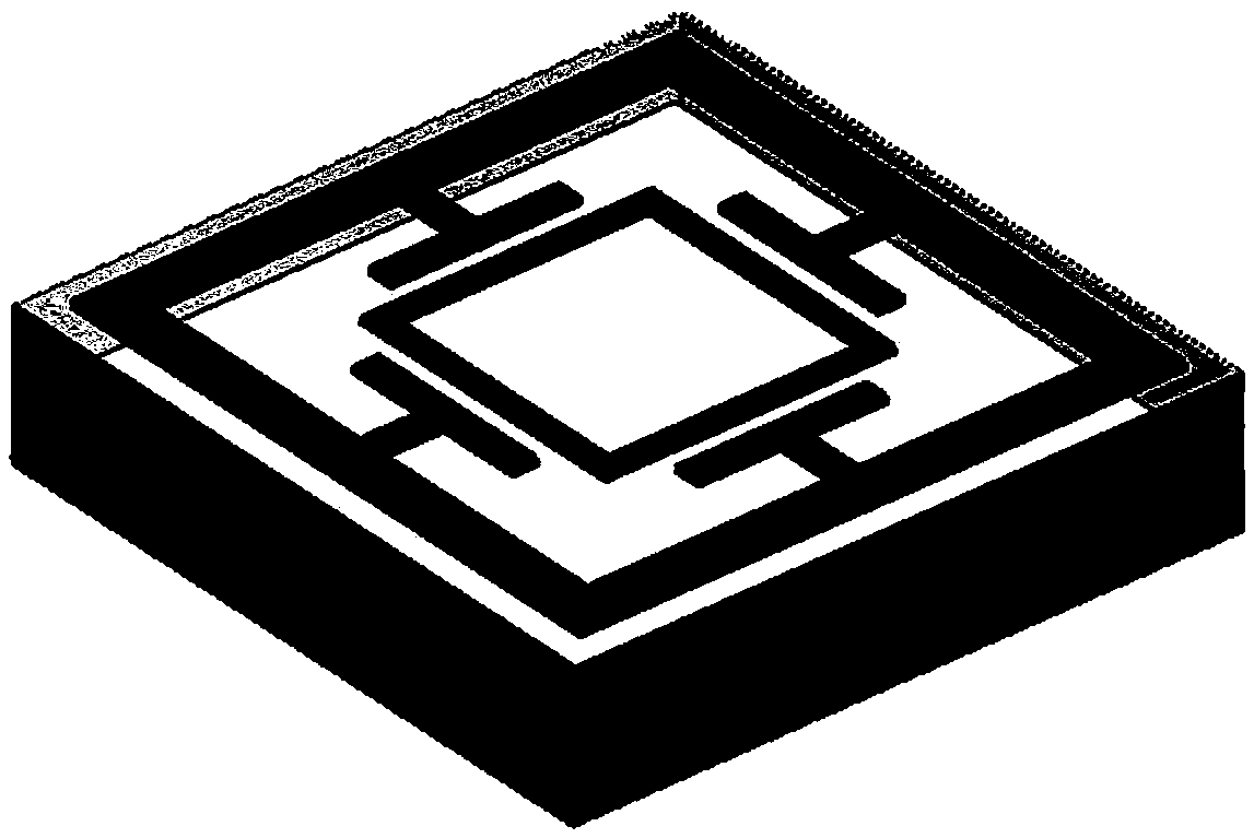
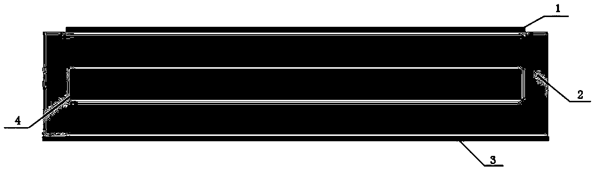
[0018] The design idea of ​​the microfluidic metamaterial structure based on PDMS encapsulation technology includes the following steps:

[0019] Combined with the conventional "sandwich" absorbing structure, the original dielectric layer is replaced by a PDMS-encapsulated microfluidic structure. The production process of the PDMS encapsulation layer is: prepare the prepolymer and the curing agent at a mass ratio of 10:1 , the preparation solution was poured on the SU-8 mold, poured into the mold and stood in a vacuum box for 12 hours, then heated on the baking table from room temperature, heated at 75°C for 4 hours to completely solidify, and demolded to obtain the bottom layer of PDMS; Prepare the prepolymer and curing agent according to the mass ratio of 15:1, stir evenly, and defoam; secondly, spin-coat the prepared solution on the silicon wafer, and heat it at 70°C for 20 minutes to partially cure it, and obtain PDMS cover sheet: Plasma treatment is performed on the botto...


PUM


Abstract

The invention belongs to novel flexible metamaterial wave absorber manufacturing field and relates to a PDMS packaging technology-based microfluid metamaterial structure. The design idea of the structure comprises the following steps that: a conventional sandwich wave absorbing structure is used in a combined manner, the original dielectric layer of the conventional sandwich wave absorbing structure is replaced with a PDMS packaged microfluid structure; the packaged microfluid is filled with a liquid having a high dielectric constant and large tangential angle loss; and a dielectric substrateand a metal pattern are sputtered to two sides of a package layer through a sputtering process, so that a flexible wave absorbing material is obtained. The process flow of the PDMS packaging technology-based microfluid metamaterial structure of the present invention is based on the PDMS package process, so that the PDMS packaging technology-based microfluid metamaterial structure can be thinner; compared with a conventional wave absorbing material structure, the PDMS packaged microfluid metamaterial wave absorber is thinner; and a material for making the wave absorber is flexible.

Description

technical field [0001] The invention belongs to the field of manufacturing novel flexible metamaterial wave absorbers, in particular to a microfluid metamaterial structure based on PDMS packaging technology. Background technique [0002] As a new type of periodic artificial electromagnetic structure, metamaterials are a hot research direction nowadays, mainly combined with technologies such as wave-absorbing materials, frequency-selective surfaces, and stealth materials. With the improvement of technological level, metamaterials are gradually applied in structures such as antennas and filters. The wave-absorbing materials that have emerged in recent years are usually realized by magnetron sputtering. The carrier of magnetron sputtering is a flexible material. The flexible material is extremely hydrophobic, so the metal adhesion is poor; although the traditional electroplating process solves the The problem of high precision and strong adhesion, but it is not easy to achieve...

Claims


Application Information

Patent Timeline
IPC IPC(8): H01Q15/00H01Q17/00
CPCH01Q15/0086H01Q17/008
Inventor 段俊萍张斌珍杨玉华刘云鹏鄢力田英
Owner ZHONGBEI UNIV
Why Eureka
Try Eureka