High-reliability planar bump type packaging method and packaging structure

A technology of planar bump type and packaging method, which is applied in the manufacture of electrical components, electrical solid devices, semiconductor/solid devices, etc. It can solve the problem of poor contact effect, small pin area, and inability to guarantee the effective gripping area of ​​metal pins, etc. problem, achieve the effect of reducing the missed brush rate, increasing the area, and improving the test UPH

Pending Publication Date: 2018-08-10
CHANGJIANG ELECTRONICS TECH CHUZHOU
View PDF1 Cites 7 Cited by
  • Summary
  • Abstract
  • Description
  • Claims
  • Application Information

AI Technical Summary

Problems solved by technology

[0009] Aiming at the problem that in the back protection process existing in the prior art, the simple ink brushing process cannot guarantee the effective gripping area of ​​the metal pin, after cutti

Method used


Image

  • High-reliability planar bump type packaging method and packaging structure
  • High-reliability planar bump type packaging method and packaging structure
  • High-reliability planar bump type packaging method and packaging structure

Examples


Embodiment 1

[0065] Such as Figure 1-8 As shown, a high-reliability planar bump packaging method uses a planar bump packaging method to set an ink layer on the redundant metal area etched on the back of the substrate after the etching step on the back of the substrate, and the ink layer 7 covers the surface of the metal area and On the side of the pins of the metal substrate 1 , the pins of the metal substrate 1 protrude from the ink layer 7 . The ink layer 7 can ensure that the short circuit caused by bridging is prevented during the welding process; welding is only performed on the parts that must be welded to avoid waste of solder; reducing copper pollution to the welding tank; preventing external environmental factors such as dust and moisture from causing Insulation deterioration and corrosion; high insulation, making it possible to increase the density of circuits. The protruding ink layer 7, after adding the pin metal layer 8, effectively increases the overall glue-grabbing area, ...

Embodiment 2

[0090] Embodiment 2 is basically the same as Embodiment 1, and furthermore, preferably, step A further includes placing the ink-brushed substrate in a vacuum box for vacuuming. When vacuuming, choose 0.08-0.1MPa, and the time is 5-10min. During the process of brushing ink, because there are air bubbles in the ink, put the substrate after brushing ink in a vacuum box for vacuuming, which can effectively prevent the product The generation of internal air bubbles ensures the quality of the product and prevents the introduction of new defects. And because of the two-step baking steps before and after, the vacuuming step also effectively prevents the cracking and unevenness of the ink layer during baking due to air bubbles during the baking stage, which affects the overall performance, and also prevents the height of the ink from being inconsistent when it shrinks. The protruding height of the pins is inconsistent, which will cause glue brushing defects in the subsequent process an...

Embodiment 3

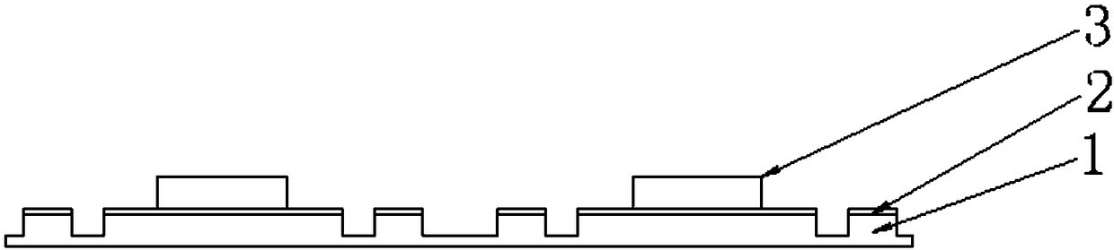
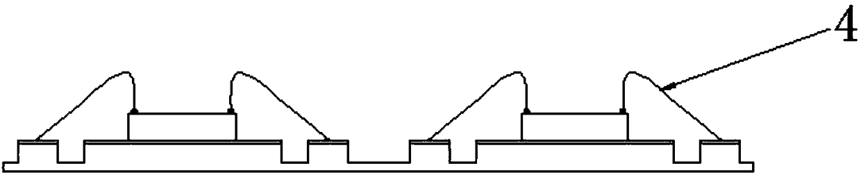
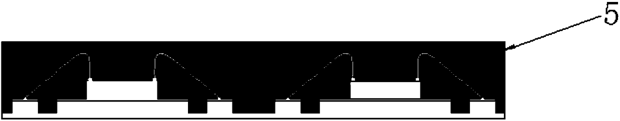
[0092] Based on the above method, a high-reliability planar bump package structure includes a chip carrier base, a wire-bonding inner pin carrier base, a chip 3, a lead 4 and a plastic package, and the chip carrier base includes a base island and a base island The front metal layer 2 of the wire-bonding inner foot base includes pins and the front metal layer 3 of the pins. There is a metal layer 2 on the connecting rib, and the chip 3 is implanted on the front metal layer 2 of the chip bearing base. 3. The front side and the front side metal layer 2 are respectively connected with the two ends of the metal wires to form a semi-finished package structure. The front side and the outer peripheral edge of the semi-finished package structure form an encapsulation 5, and make the base island and the back of the pin protrude from the surface of the plastic package. The base island and pin surface on the back are plated with pin metal layer 8 , except that the extra metal area on the b...


PUM


Abstract

The invention discloses a high-reliability planar bump type packaging method and a packaging structure, and belongs to the field of semiconductor packaging. In the back protection process existing inthe prior art, a simple ink brushing process cannot ensure the effective glue gripping area of metal pins, the area of the pins is small after cutting, and the problem of poor probe contact effect issolved. The high-reliability planar bump type packaging method and the packaging structure are provided, the packaging structure includes a chip bearing base, a wire bonding inner lead bearing base, chips, lead wires and a plastic package body, the chip bearing base comprises base islands and front metal layers of the base islands, the wire bonding inner lead bearing base comprises pins and frontmetal layers of the pins, and an excess metal area, except the back face of a pin metal layer, is provided with an ink layer. A good glue gripping effect is achieved, the contact defect rate is low, the contact effect is good and the detection rate is high during the detection of finished products.

Description

technical field [0001] The invention relates to the field of semiconductor packaging, more specifically, to a high-reliability planar bump packaging method and packaging structure. Background technique [0002] For decades, integrated circuit packaging technology has been following the development of integrated circuits, and people have been looking for the best balance between small size and high performance. From the DIP plug-in package in the 1970s to the SOP surface mount package, and then to the QFP flat chip package in the 1980s, the package volume of the chip has been developing towards miniaturization, and the structural performance has been continuously improved. In the 1990s, the QFN four-sided flat package appeared, based on the QFP, the output pins around the package body were retracted to the bottom of the package body, thereby greatly reducing the occupied space during the placement operation. However, QFN often has problems such as unstable inner solder joint...

Claims


Application Information

Patent Timeline
IPC IPC(8): H01L21/48H01L21/56H01L21/60H01L23/31H01L23/49H01L23/492
Inventor 吴奇斌吴靖宇范荣定吴莹莹吴涛吕磊汪阳
Owner CHANGJIANG ELECTRONICS TECH CHUZHOU
Why Eureka
Try Eureka