hemt device and its preparation method

A device and cap layer technology, applied in the field of microelectronics, can solve the problems of low repeatability, unsatisfactory effect, high time consumption, etc., achieve excellent stress behavior, good metal adhesion, and improve device reliability.

Active Publication Date: 2020-10-02
XIDIAN UNIV
View PDF6 Cites 0 Cited by
  • Summary
  • Abstract
  • Description
  • Claims
  • Application Information

AI Technical Summary

Problems solved by technology

However, this method is time-consuming, costly and has low reproducibility, and is not yet widely used
[0007] To sum up, at present, the method of realizing waterproof and oxygen prevention of AlGaN / GaNHEMT devices at home and abroad mainly adopts silicon nitride passivation technology, and the effect is not ideal.

Method used


Image

  • hemt device and its preparation method
  • hemt device and its preparation method
  • hemt device and its preparation method

Examples


Embodiment 1

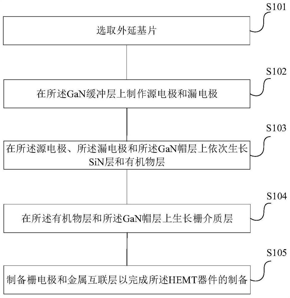
[0028] See figure 1 , figure 1 A schematic flow chart of a preparation method for a HEMT device provided in an embodiment of the present invention, including:

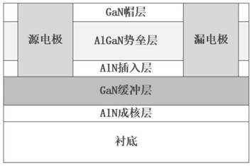
[0029] S101. Select an epitaxial substrate; the epitaxial substrate sequentially includes a substrate, a nucleation layer, a GaN buffer layer, an AlN insertion layer, an AlGaN barrier layer, and a GaN cap layer from bottom to top;

[0030] S102, forming a source electrode and a drain electrode on both ends of the GaN buffer layer;

[0031] S103, sequentially growing a SiN layer and an organic layer on the source electrode, the drain electrode, and the GaN cap layer to form a passivation layer;

[0032] S104, growing a gate dielectric layer on the organic layer and the GaN cap layer;

[0033] S105 , preparing a gate electrode and a metal interconnection layer to complete the preparation of the HEMT device.

[0034] Preferably, S102 may include:

[0035] S1021, photoetching a source electrode region and a drain elec...

Embodiment 2

[0054] Please refer to Figure 2a-2i , Figure 2a-2i The schematic flow chart of the preparation process of a HEMT device provided by the embodiment of the present invention, this embodiment describes the preparation method of the HEMT device of the present invention in detail on the basis of the first embodiment. include:

[0055] S201, such as Figure 2a As shown, the source and drain electrodes are fabricated on the GaN buffer layer of the epitaxial substrate.

[0056] Among them, the epitaxial substrate can be the initially purchased epitaxial substrate, or it can be the manufactured epitaxial substrate, and the epitaxial substrate includes substrate, nucleation layer, GaN buffer layer, AlN insertion layer, AlGaN potential barrier layer and GaN cap layer.

[0057] Specifically, the substrate is made of sapphire material.

[0058] S2011, photoetching the source electrode region and the drain electrode region on the GaN cap layer:

[0059] First, bake the epitaxial sub...

Embodiment 3

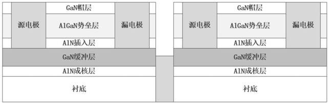
[0137] Further, please refer to image 3 , image 3 The schematic flow chart of another HEMT device manufacturing method provided by the embodiment of the present invention is described in detail in this embodiment on the basis of the first embodiment. Specifically include:

[0138] S301, fabricating a source electrode and a drain electrode on an epitaxial substrate.

[0139] Among them, the epitaxial substrate can be the initially purchased epitaxial substrate, or it can be the manufactured epitaxial substrate, and the epitaxial substrate includes substrate, nucleation layer, GaN buffer layer, AlN insertion layer, AlGaN potential barrier layer and GaN cap layer.

[0140] Specifically, the substrate is a SiC substrate.

[0141] S3011, photoetching a source electrode region and a drain electrode region on the GaN cap layer:

[0142] S3012, evaporating the source electrode and the drain electrode on the GaN cap layer in the source electrode region and the drain electrode re...


PUM

PropertyMeasurementUnit
depthaaaaaaaaaa
thicknessaaaaaaaaaa
thicknessaaaaaaaaaa

Abstract

The invention relates to a HEMT (high electron mobility transistor) device and a preparation method. The preparation method includes: S101, selecting an epitaxial substrate which sequentially comprises a substrate, a nucleating layer, a GaN buffering layer, an AlN inserting layer, a AlGaN potential barrier layer and a GaN cap layer from bottom to top; S102, making a source electrode and a drain electrode on the GaN buffering layer; S103, sequentially growing a SiN layer and an organic matter layer on the source electrode, the drain electrode and the GaN cap layer to form a passivation layer; S104, growing a gate medium layer on the organic matter layer and the GaN cap layer; S105, preparing a gate electrode and a metal interconnection layer to complete preparation of the HEMT device. The BCB organic matter layer is grown on the grown SiN layer, so that the device has low hygroscopicity, excellent stress behavior and good metal adhesiveness, and reliability of the device can be improved.

Description

technical field [0001] The invention belongs to the technical field of microelectronics, and in particular relates to a HEMT device and a preparation method thereof. Background technique [0002] With the improvement of technology level, the existing first and second generation semiconductor materials can no longer meet the needs of higher frequency and higher power electronic devices, while electronic devices based on nitride semiconductor materials can meet this requirement, greatly improving device performance. Due to the high two-dimensional electron gas density and high electron mobility in the AlGaN / GaN heterostructure, it has very good application prospects in high-power microwave devices. [0003] Passivation of AlGaN / GaN is particularly important because there are Al and Ga atoms combined with oxygen on the surface of AlGaN / GaN first-generation high electron mobility transistors (High Electron Mobility Transistor, HEMT), which reduces the concentration of two-dimen...

Claims


Application Information

Patent Timeline
Patent Type & Authority Patents(China)
IPC IPC(8): H01L29/778H01L21/335H01L23/29
CPCH01L23/291H01L23/293H01L29/66462H01L29/7786
Inventor 马晓华郝跃陈丽香祝杰杰刘捷龙
Owner XIDIAN UNIV
Why Eureka
Try Eureka