High-reliability double-sided battery and preparation method thereof
A bifacial battery and reliable technology, applied in the field of solar cells, can solve the problems of unsatisfactory improvement of the PID attenuation phenomenon on the back of the double-sided battery, PID on the back of the double-sided battery restricts the promotion of double-sided PERC products, etc.
- Summary
- Abstract
- Description
- Claims
- Application Information
AI Technical Summary
Problems solved by technology
Method used
Image
Examples
Embodiment 1
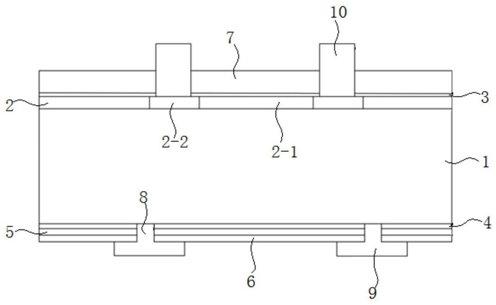
[0054] Such as figure 1As shown, the back battery of this embodiment includes a silicon wafer substrate 1, and the back surface of the silicon wafer substrate 1 is sequentially provided with a silicon oxide protective layer 4, an aluminum oxide passivation layer 5, and a silicon nitride passivation and protective layer 6. , wherein the silicon oxide protective layer 4 is deposited by ALD, and its specific preparation process is as follows: put the silicon wafer into the atomic layer deposition chamber, heat the silicon wafer substrate to a temperature of 150°C, and evacuate the reaction chamber until the pressure reaches When the temperature is 20mbar or below, feed tris(dimethylamino)silane (silicon-based precursor) with a flow rate of 150 sccm for 4s; then purge with nitrogen for 20s; Purge for 10s; repeat the above steps 20 times to prepare a silicon oxide protective film of about 2nm.
Embodiment 2
[0056] The rear cell of this embodiment comprises a silicon wafer base 1, and the front side of the silicon wafer base 1 is provided with a front emitter 2, a front oxide layer 3, a front silicon nitride passivation and anti-reflection layer 7, and a positive electrode 10 in sequence from bottom to top. , and its back is sequentially provided with a silicon oxide protective layer 4 , an aluminum oxide passivation layer 5 , a silicon nitride passivation and protective layer 6 and a rear sub-gate electrode 9 from inside to outside.
[0057] The preparation process of the rear battery in this embodiment includes the following steps:
[0058] 1. Texture making: use single crystal P-type silicon wafer substrate 1, and use alkali to make texturing on the front and back to form a textured structure.
[0059] 2. Diffusion: React the silicon wafer after texturing with phosphorus oxychloride and the silicon wafer at high temperature, so that the front diffuses to form a PN emitter junct...
Embodiment 3
[0078] The structure of the back battery of this embodiment is the same as that of Example 2, and the preparation method of the back battery of this embodiment specifically includes the following process steps:
[0079] 1. Texture making: Single crystal P-type silicon wafers are used, and alkali is used to make texturing on the front and back to form a textured structure.
[0080] 2. Diffusion: React the silicon wafer after texturing with phosphorus oxychloride and the silicon wafer at high temperature to make the front diffuse to form a PN emitter junction 2 . Diffusion is carried out by the above-mentioned diffusion process, and the square resistance of the thin layer on the front surface after diffusion is between 150Ω / □.
[0081] 3. Laser SE: use the diffused phosphosilicate glass as the phosphorus source, and perform laser doping on the front side of the diffused silicon wafer and the metallized area corresponding to the positive electrode grid line to form a heavily dope...
PUM
| Property | Measurement | Unit |
|---|---|---|
| thickness | aaaaa | aaaaa |
| thickness | aaaaa | aaaaa |
| thickness | aaaaa | aaaaa |
Abstract
Description
Claims
Application Information
