Method for producing wafer

A wafer and single crystal technology, applied in the field of wafer generation, can solve problems such as poor production efficiency and difficulty in wafer peeling, and achieve the effect of realizing productivity

Pending Publication Date: 2018-08-24
DISCO CORP
View PDF9 Cites 7 Cited by
  • Summary
  • Abstract
  • Description
  • Claims
  • Application Information

AI Technical Summary

Problems solved by technology

However, it is difficult to peel the wafer from the peeling laye

Method used


Image

  • Method for producing wafer
  • Method for producing wafer
  • Method for producing wafer

Examples


Example Embodiment

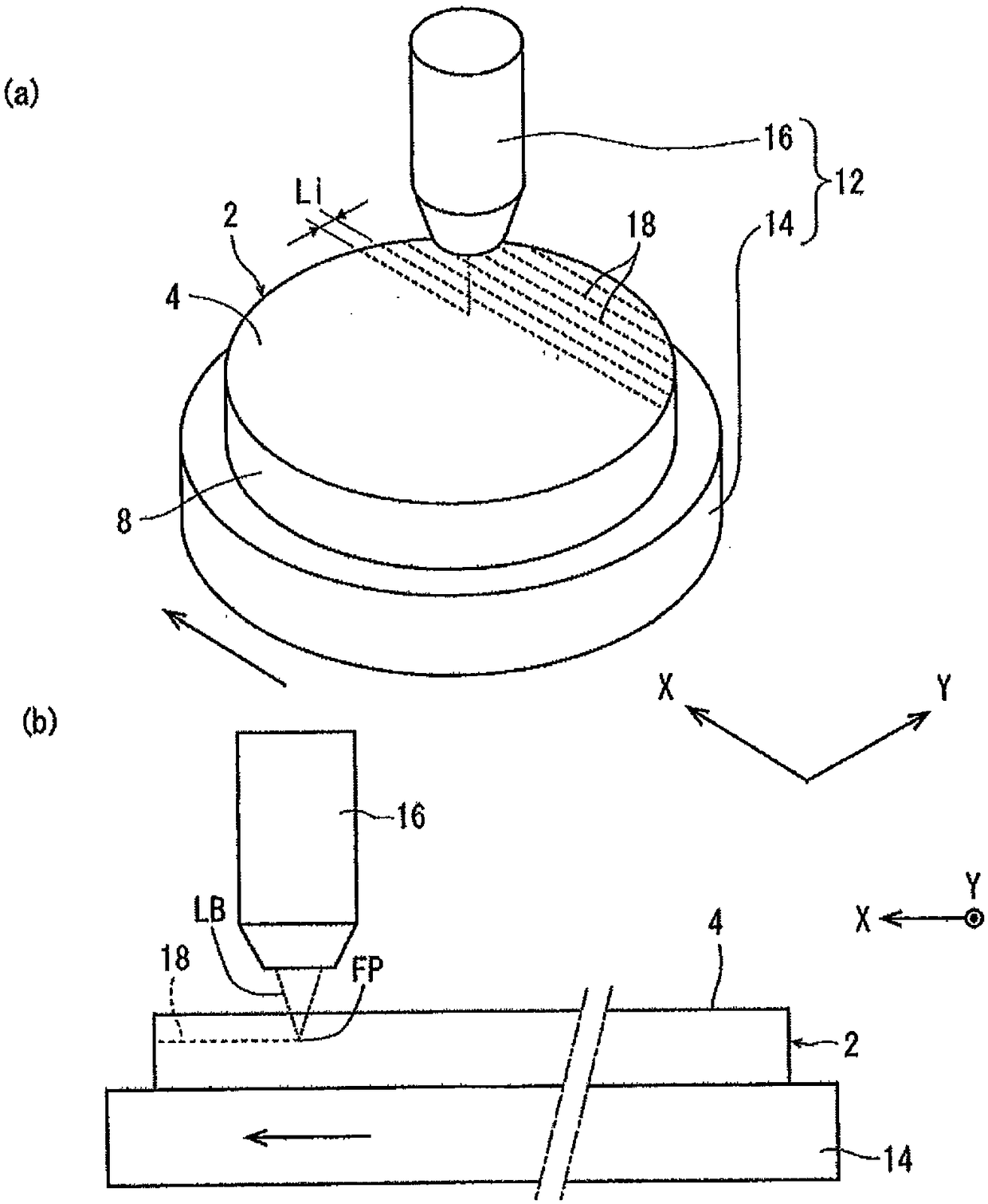
[0028] Regardless of whether the c-axis of the single crystal SiC ingot is inclined with respect to the vertical line of the end face, the wafer production method of the present invention can be used. First, refer to Figure 1 to Figure 8 , an embodiment of the wafer production method of the present invention under a single crystal SiC ingot in which the vertical line of the end face coincides with the c-axis will be described.

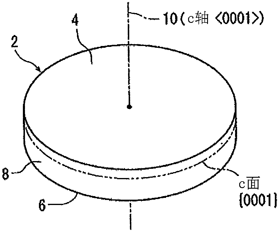
[0029] figure 1 The illustrated cylindrically shaped hexagonal single crystal SiC ingot 2 (hereinafter referred to as "ingot 2") has: a circular-shaped first face 4 (end face); a circular-shaped second face 6, which is in the first Opposite side of face 4; peripheral face 8, which is located between first face 4 and second face 6; c-axis ( direction), which runs from first face 4 to second face 6; and c-face ({{ 0001} plane), which is perpendicular to the c-axis. In the ingot 2, the c-axis is not inclined with respect to the vertical line 10 of the f...


PUM


Abstract

The present invention provides a method for producing a wafer capable of effectively stripping the wafer from a single crystal SiC crystal ingot. The method at least comprises the following steps of:a stripping layer formation process: locating a focus (FP) of a laser light (LB) having a wavelength of permeability about the single crystal SiC at the depth having a thickness of a wafer to be generated far away from a first surface (4) (end face) of the crystal ingot (2) to perform radiation of the laser light (LB) for the crystal ingot (2) to form a stripping layer (22), wherein the strippinglayer (22) is formed by an improvement portion (18) of separating the SiC into Si and C and cracks (20) formed in a isotropy mode at a c surface from the improvement portion (18); a stripping open endformation process configured to perform further radiation of the laser light (LB) to one part of all of the periphery area of the periphery area of the stripping layer (22) to allow the cracks (20) to grow to form the stripping open end (23); and a wafer generation process configured to steep the crystal ingot (2) into the liquid (26) to give ultrasonic waves having frequency larger than the frequency being similar to the natural vibration frequency of the crystal ingot (2) so as to strip one part of the crystal ingot (2) to generate the wafer (34) by taking the stripping layer (22) as an interface.

Description

technical field [0001] The present invention relates to a wafer generation method that generates wafers from a single crystal SiC ingot. Background technique [0002] IC, LSI, LED and other devices are based on Si (silicon), Al 2 O 3 It is formed by laminating a functional layer on the front surface of a wafer made of (sapphire) or the like as a raw material and dividing it by a line to divide. In addition, power devices, LEDs, and the like are formed by laminating a functional layer on the front surface of a wafer made of single crystal SiC (silicon carbide) and dividing it by predetermined dividing lines. The wafer on which the devices are formed is processed by a cutting device or a laser processing device on the lines to be divided to be divided into individual devices, and each of the divided devices is used in electrical equipment such as mobile phones and personal computers. [0003] Device-forming wafers are typically produced by thinly slicing a cylindrical ingot...

Claims


Application Information

Patent Timeline
IPC IPC(8): H01L21/02
CPCH01L21/02H01L21/0201H01L21/78H01L21/76H01L21/02598H01L21/02378H01L21/324B23K26/38
Inventor 平田和也山本凉兵
Owner DISCO CORP
Why Eureka
Try Eureka