Wafer carrier, wafer cleaning system and method

A cleaning system and wafer technology, applied in the manufacturing of electrical components, circuits, semiconductor/solid-state devices, etc., can solve the problem of not being able to meet the requirements of unconventional thickness wafer cleaning specifications, reducing wafer yield, affecting product yield, etc. problems, to avoid flyer breakage, improve yield, and enhance compatibility

Active Publication Date: 2020-12-04
NAT CENT FOR ADVANCED PACKAGING CO LTD
View PDF6 Cites 0 Cited by
  • Summary
  • Abstract
  • Description
  • Claims
  • Application Information

AI Technical Summary

Problems solved by technology

In the above process, due to the warping of the wafer, it is easy to slip and break during the transfer process, and in the cleaning process, because the wafer is directly adsorbed on the chuck, it is very easy to cause the wafer to fly due to weak vacuum adsorption. chip breakage, thus affecting product yield
[0004] At the same time, the existing single-chip cleaning equipment can only clean wafers with conventional thickness. The so-called conventional thickness generally refers to the thickness value between 500μm-1mm, and cannot meet the requirements of unconventional thickness (less than 500μm or greater than 1mm). Wafer Cleaning Specifications
If cleaning equipment with mismatched thickness specifications is used for cleaning, the possibility of wafer fragmentation in the cleaning chamber will be significantly increased, thereby greatly reducing the yield of wafers

Method used


Image

  • Wafer carrier, wafer cleaning system and method
  • Wafer carrier, wafer cleaning system and method
  • Wafer carrier, wafer cleaning system and method

Examples


Embodiment 1

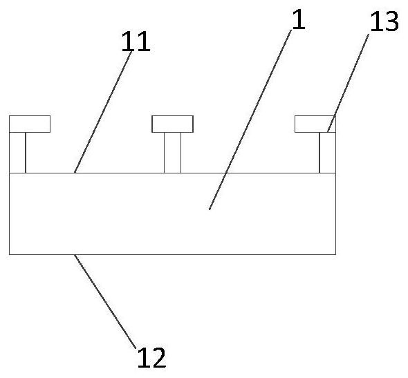
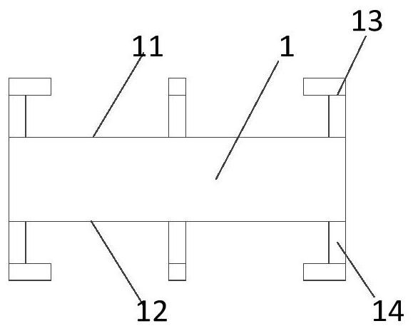
[0048] An embodiment of the present invention provides a wafer carrier, such as figure 1As shown, the carrier body 1 is included, and the carrier body 1 has a relative carrying surface 11 and a fixed surface 12; the carrying surface 11 is used to carry the wafer, and the fixed surface 12 is used to fix the carrier; the edge of the carrying surface 11 is also provided with Several first clamps 13 for fixing the wafer. Wherein, both the carrying surface 11 and the fixing surface 12 are smooth surfaces, and the size of the carrying surface 11 is adapted to the size of the wafer.

[0049] As an alternative embodiment, the size of the carrying surface 11 may not be adapted to the size of the wafer, and the first clamp 13 may not be arranged on the edge of the carrying surface 11, but be arranged on the carrying surface 11 to adapt to the size of the wafer. Periphery of the area, as long as the first clamper 13 can clamp the wafer.

[0050] In this embodiment, the fixed surface 12...

Embodiment 2

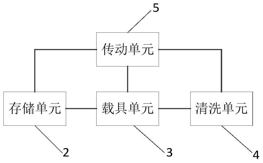
[0055] Embodiments of the present invention provide a wafer cleaning system, such as image 3 As shown, it includes a storage unit 2 , a carrier unit 3 , a cleaning unit 4 and a transmission unit 5 . Wherein, the storage unit 2 is used to store the wafer; the carrier unit 3 is used to store the carrier provided in the above-mentioned embodiment 1; the cleaning unit 4 is used to clean the wafer loaded on the carrier, wherein the fixed surface 12 fixed on the chuck in the cleaning unit 4;

[0056] The setting of the carrier unit 3 can store the carrier on the one hand, and on the other hand provides a platform for loading the wafer on the carrier. When the wafer is loaded on the carrier, the two form a whole and are transported by the transmission unit 5 To the cleaning unit 4, the whole is cleaned, thereby ensuring the safety of the wafer during the transfer process and during the cleaning process, and the flying pieces are not easy to be broken.

[0057] As a preferred embod...

Embodiment 3

[0060] Embodiments of the present invention provide a wafer cleaning method, such as Figure 5 shown, including the following steps:

[0061] Step S31 , the wafer to be cleaned is transferred from the storage unit 2 to the carrier unit 3 by the transmission unit 5 , and the wafer is loaded on the carrier. Specifically, the wafer to be cleaned is picked up from the storage unit 2 by a manipulator and transferred to the carrier unit 3. In the carrier unit 3, the installation of the wafer and the carrier is realized. The installation process can be manual or can be It is an automated operation.

[0062] Step S32 , transferring the wafer to the cleaning unit 4 through the transmission unit 5 . This step transfers the wafer and the carrier as a whole.

[0063] Step S33 , fixing the fixing surface 12 of the carrier on the chuck in the cleaning unit 4 to clean the wafer. Wherein, the fixing surface 12 of the carrier can be fixed by clamps, by vacuum adsorption, by magnetic adsorp...


PUM

PropertyMeasurementUnit
thicknessaaaaaaaaaa
thicknessaaaaaaaaaa
thicknessaaaaaaaaaa

Abstract

The invention relates to the technical field of a semiconductor, and discloses a wafer carrier, and a wafer cleaning system and method. The wafer carrier comprises a carrier body, and the carrier bodyhas opposite bearing surface and fixing surface; the bearing surface is used for bearing wafers and the fixing surface is used for fixing the carrier; and a plurality of first clamps for fixing wafers are arranged on the edge of the bearing surface. When the wafers are cleaned, the wafers are pre-fixed on the bearing surface of the carrier, and then the fixing surface of the carrier is fixed in acleaning cavity; in the cleaning process, the wafers are firmly fixed on the carrier without being fixed in the cleaning cavity directly, so that wafer cracking caused by infirm wafer adsorption dueto that the wafers are directly adsorbed in the cleaning cavity in the conventional mode can be avoided, and wafer finished product rate is improved; and in addition, when the wafers are transported on a cleaning assembly line, the wafers also can be fixed on the carrier, so that safety of the wafers in the transporting process can be further ensured.

Description

technical field [0001] The invention relates to the technical field of semiconductors, in particular to a wafer carrier, a wafer cleaning system and method. Background technique [0002] Wafer refers to the silicon wafer used in the production of silicon semiconductor integrated circuits. Because of its circular shape, it is called a wafer. As the feature size of integrated circuits enters the deep sub-micron stage, the cleanliness of the wafer surface required in the integrated circuit wafer manufacturing process is becoming more and more stringent. Therefore, in the semiconductor manufacturing process, wafer cleaning is a very important link. [0003] The existing wafer cleaning process usually includes the following steps: Step 1, the wafer is directly grasped by the robot and transferred between the units; Step 2, when it reaches the cleaning unit, the wafer is directly adsorbed on the chuck in the cleaning chamber; Step 3, further cleaning the wafer. In the above pro...

Claims


Application Information

Patent Timeline
Patent Type & Authority Patents(China)
IPC IPC(8): H01L21/687H01L21/67
CPCH01L21/67028H01L21/68721
Inventor 李恒甫
Owner NAT CENT FOR ADVANCED PACKAGING CO LTD
Why Eureka
Try Eureka