Antimony selenide thin film preparation method and device

A thin film preparation and antimony selenide technology, which is applied in the field of preparation of antimony selenide photoelectric thin film materials, can solve the problems of increasing production links and production costs, poor post-selenization selenium supplementation process effect, unfriendly environment, etc., and achieves favorable Production technology, reduction of preparation and production costs, environmental friendliness

Inactive Publication Date: 2018-09-04
HEBEI UNIVERSITY
View PDF1 Cites 4 Cited by
  • Summary
  • Abstract
  • Description
  • Claims
  • Application Information

AI Technical Summary

Problems solved by technology

[0006] One of the purposes of the present invention is to provide a preparation method of antimony selenide thin film, to solve the problem that the existing antimony selenide thin film needs to introduce additional selen

Method used


Image

  • Antimony selenide thin film preparation method and device
  • Antimony selenide thin film preparation method and device
  • Antimony selenide thin film preparation method and device

Examples


Embodiment 1

[0022] Example 1 Antimony Selenide Film Online Selenium Compensation Device

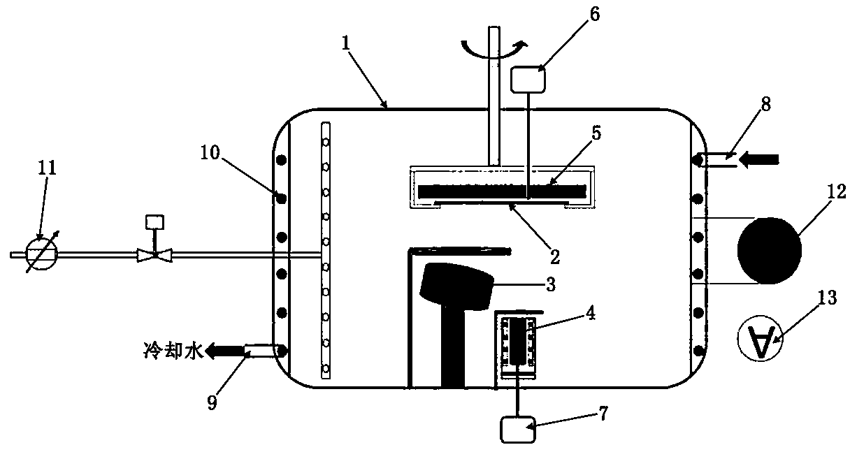
[0023] The device structure of the present invention is as figure 1 As shown, the growth chamber 1 is provided with a sputtering system and a thermal evaporation system respectively.

[0024] The sputtering system is provided with a rotating substrate table with a heating wire 5 in the growth chamber 1, a radio frequency magnetron sputtering target table is provided under the substrate table, and a cooling system is provided on the peripheral wall of the growth chamber 1, for The growth chamber 1 is fed with an intake system of inert Ar gas, a vacuum system and a pressure detection system. The rotating substrate table is used to place the substrate 2 to be sputtered, and the heating wire 5 is used to heat the substrate 2 placed on the rotating substrate table, and monitor the temperature of the substrate 2 in real time through the first thermometer 6 . The radio frequency magnetron sputtering targe...

Embodiment 2

[0026] Example 2 Application of the method of the present invention to prepare antimony selenide thin film solar cells

[0027] The steps of preparing antimony selenide thin film solar cells with online selenium compensation are as follows:

[0028] (1) Substrate preparation

[0029] Using glass as a substrate, first soak the glass in an electronic cleaner solution for 12 hours, then take it out, rinse it with a large amount of deionized water, and blow it dry with nitrogen.

[0030] (2) Deposit molybdenum back electrode layer

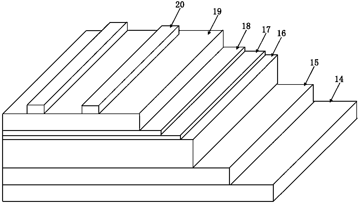
[0031] The molybdenum (Mo) back electrode layer was prepared by magnetron sputtering technology: Ar gas was used as the reaction gas, the sputtering pressure was 0.4Pa, and the sputtering power density was about 4W / cm 2 , the thickness of the prepared molybdenum back electrode film is about 700nm, and its resistivity is about 3×10 -5 Ω·cm.

[0032] (3) Deposition of p-type antimony selenide semiconductor layer

[0033] Select the radio frequency m...

Embodiment 3

[0047] Select a glass substrate deposited with a Mo film with a thickness of 700nm as the substrate, and prepare an antimony selenide film with online selenium compensation:

[0048] (1) Using radio frequency magnetron sputtering process (sputtering power density is 1.5W / cm 2 , sputtering pressure 0.5Pa), using a circular antimony selenide target with a diameter of 10 cm in line with the stoichiometric ratio as the sputtering target, using Ar gas as the sputtering gas to sputter and deposit the antimony selenide layer on the substrate;

[0049] The deposition time of this step is set as 14min, and the thickness of the obtained antimony selenide layer is about 700nm,

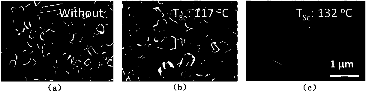
[0050] (2) While sputtering and depositing the antimony selenide layer in step (1), a thermal evaporation process is used to perform selenium compensation online with high-purity (purity 99.99%) selenium particles as the evaporated selenium source.

[0051] In this example, 2 groups of parallel experiments and 1...


PUM

PropertyMeasurementUnit
Thicknessaaaaaaaaaa
Thicknessaaaaaaaaaa

Abstract

The invention discloses an antimony selenide thin film preparation method and device. According to the method of the of the present invention, a solid selenium source is evaporated in the cavity of agrowth chamber during a process of applying a sputtering method to prepare an antimony selenide thin film, so that on-line selenium compensation can be realized, and therefore, the components of the thin film can be optimized; parameters such as temperature of the evaporation of the selenium source are adjusted, so that the chemical components of the antimony selenide thin film can be adjusted tosatisfy a stoichiometric ratio, and therefore, the problem of the selenium deficiency of the antimony selenide thin film prepared by the sputtering method can be solved. The device of the present invention is provided with a sputtering system and a thermal evaporation system, wherein the sputtering system and thermal evaporation system are arranged in the growth chamber; the sputtering system is provided with a rotating substrate table, a sputtering target, a cooling system, an air intake system, a vacuum-pumping system and a gas pressure detection system, wherein the rotating substrate tableis provided with a heating wire, the sputtering target is disposed under the substrate table, the rotating substrate table and the sputtering target are arranged in the growth chamber, the cooling system, the air intake system, the vacuum-pumping system and the gas pressure detection system are disposed on the growth chamber; the thermal evaporation system is provided with a thermal evaporation crucible for holding the solid selenium source, wherein the thermal evaporation crucible is arranged in the growth chamber.

Description

technical field [0001] The invention relates to the preparation of an antimony selenide photoelectric thin film material, in particular to an on-line selenium compensation method and device for an antimony selenide thin film. Background technique [0002] Antimony Selenide (Sb 2 Se 3 ) is a binary compound material with a bandgap of about 1.2eV and an absorption coefficient of about 10 5 cm -1 , is a very ideal photovoltaic material, its theoretical efficiency can reach 30%, and because of its abundant reserves and non-polluting characteristics to the environment, antimony selenide solar cells have broad application prospects. [0003] The common preparation methods of antimony selenide thin film are sputtering method, evaporation method and solution spin coating method, and sputtering method is rarely used. Coating method, when the antimony selenide thin film is prepared by sputtering method, the selenium deficiency of the prepared film is obvious, which causes the film...

Claims


Application Information

Patent Timeline
IPC IPC(8): H01L31/0445H01L31/0392C23C14/35
CPCY02E10/50H01L31/0445C23C14/35H01L31/0392
Inventor 李志强梁晓杨麦耀华陈静伟李刚
Owner HEBEI UNIVERSITY
Why Eureka
Try Eureka