Inorganic perovskite light emitting diode and preparation method thereof

A technology of light-emitting diodes and inorganic calcium, which is applied in semiconductor/solid-state device manufacturing, electrical components, electric solid-state devices, etc., can solve the problems of perovskite layer leakage and non-radiative recombination, so as to improve external quantum efficiency and reduce non-radiative recombination The effect of centering and suppressing generation

Inactive Publication Date: 2018-09-07
INST OF SEMICONDUCTORS - CHINESE ACAD OF SCI
View PDF5 Cites 12 Cited by
  • Summary
  • Abstract
  • Description
  • Claims
  • Application Information

AI Technical Summary

Problems solved by technology

[0004] The main purpose of the present invention is to provide an inorganic perovskite light-emitting diode and its preparation method to solve the problems of serious leakage and non-radiative recombination between the perovskite and the electron or hole injection layer and the perovskite layer itself

Method used


Image

  • Inorganic perovskite light emitting diode and preparation method thereof
  • Inorganic perovskite light emitting diode and preparation method thereof
  • Inorganic perovskite light emitting diode and preparation method thereof

Examples


Embodiment Construction

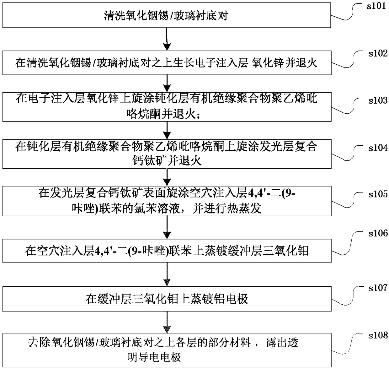
[0067] In order to make the object, technical solution and advantages of the present invention clearer, the present invention will be further described in detail below in conjunction with specific embodiments and with reference to the accompanying drawings.

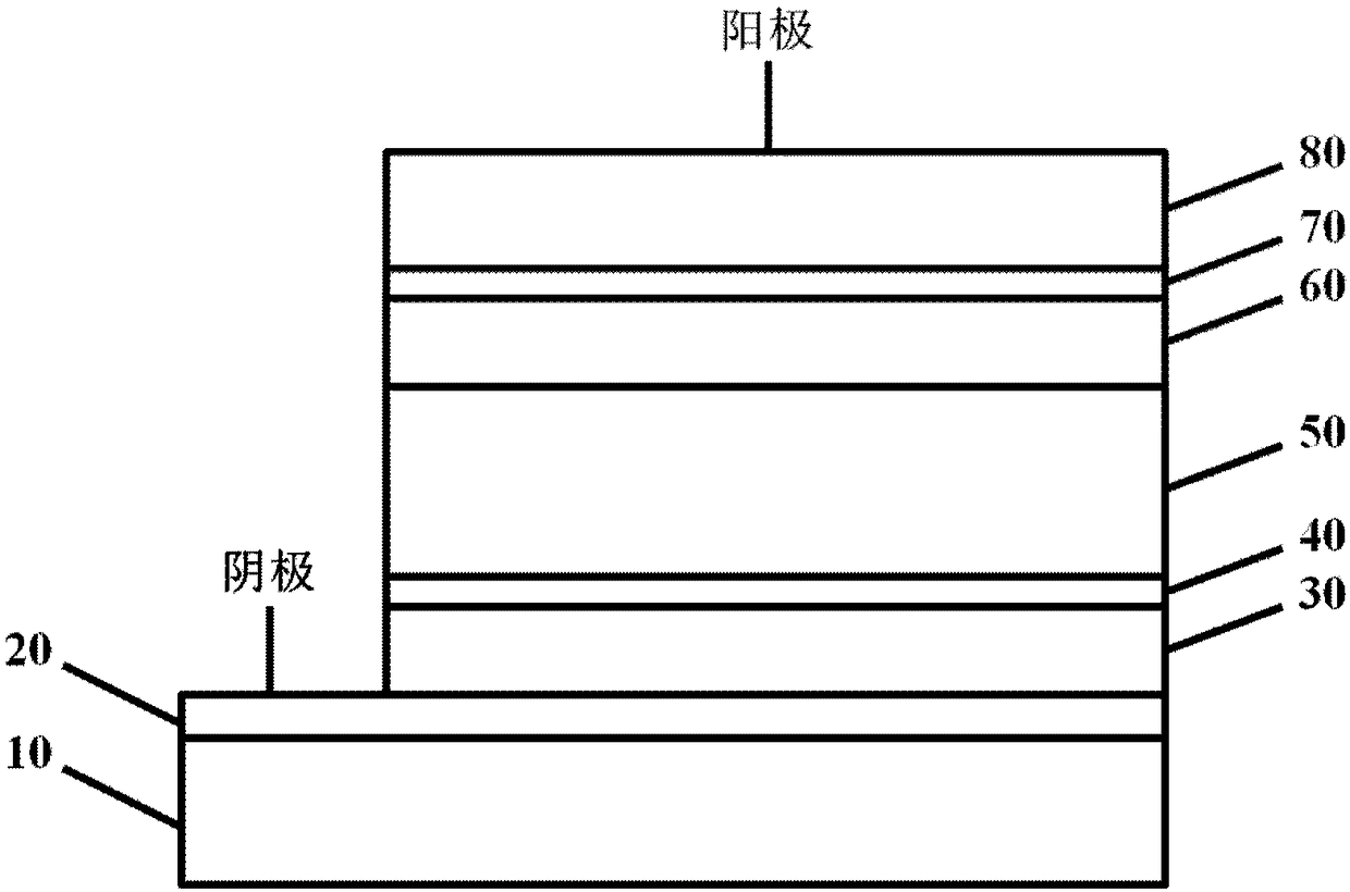
[0068] figure 1 It is a schematic structural diagram of a perovskite light-emitting diode according to an embodiment of the present invention, as figure 1 As shown, the inorganic perovskite light-emitting diode includes: a substrate 10, and a transparent conductive electrode 20 on the substrate, forming a pair of substrate 10 / transparent conductive electrode 20; a pair of substrate 10 / transparent conductive electrode 20 is sequentially placed on one end The electron injection layer 30, the passivation layer 40, the light emitting layer 50, the hole injection layer 60, the buffer layer 70 and the metal conductive electrode 80, the transparent conductive electrode 20 is the cathode, and the metal conductive electrode 80 is ...


PUM

PropertyMeasurementUnit
thicknessaaaaaaaaaa
thicknessaaaaaaaaaa

Abstract

The invention discloses an inorganic perovskite light emitting diode and a preparation method thereof. According to the method, a passivation layer (PVP) not only can improve the surface morphology ofthe perovskite and reduce the leakage current of the light emitting diode, but also can passivate surface defects of zinc oxide (ZnO), reduce the non-radiative recombination at the interface betweenthe perovskite and the zinc oxide and thus improve the radiative recombination efficiency, and can also improve the injection balance between electrons and holes at the same time. In addition, a composite perovskite light emitting material (Cs0.87MA0.13PbBr3) which is almost hole-free and very compact can be obtained by doping a small amount of MABr into CsPbBr3, thereby being also capable of effectively suppressing the generation of a non-radiative recombination center of elementary lead in CsPbBr3 while reducing the leakage current. The external quantum efficiency of the perovskite light emitting diode can be effectively improved according to the invention.

Description

technical field [0001] The invention relates to the technical field of semiconductor optoelectronic devices, in particular to an inorganic perovskite light-emitting diode and a preparation method thereof. Background technique [0002] Organic-inorganic composite perovskite materials have attracted much attention due to their advantages such as low preparation cost, simple process, wide-range adjustable band gap, high absorption coefficient, and flexible devices. At present, the efficiency of perovskite solar cells has reached 22.1%, which is almost the same as that of cells made of traditional semiconductor materials. In addition, researchers have found that perovskite materials have high fluorescence quantum efficiency (even more than 90% in the nanocrystalline state), and the color is very pure (half-peak width is about 20nm), which has great development in light-emitting diodes. potential. Compared with the traditional organic-inorganic composite perovskite, the pure in...

Claims


Application Information

Patent Timeline
Patent Type & Authority Applications(China)
IPC IPC(8): H01L51/54H01L51/50H01L51/52H01L51/56
CPCH10K85/30H10K50/171H10K50/84H10K71/00
Inventor 张留旗游经碧张兴旺尹志岗
Owner INST OF SEMICONDUCTORS - CHINESE ACAD OF SCI
Why Eureka
Try Eureka