
Dual-mode millimeter wave broadband stacking low noise amplifier with low power consumption and high linearity

A low-noise amplifier and low-noise amplification technology, which is applied in the design field of low-power and high-linearity dual-mode millimeter-wave broadband stacked low-noise amplifiers, can solve the problem that the mutual constraints of low power consumption and high linearity indicators cannot be well resolved, Improve chip cost, deteriorate RF characteristics, etc., to achieve the effect of ultra-wideband noise matching, good input and output matching, and simplifying the power supply structure

Pending Publication Date: 2018-09-25
CHENGDU GANIDE TECH
View PDF9 Cites 7 Cited by
  • Summary
  • Abstract
  • Description
  • Claims
  • Application Information

AI Technical Summary

Problems solved by technology

[0005] (1) The current multiplexing structure requires the use of feed inductance and large capacitance to achieve static bias multiplexing of two common source (or common emitter) amplifiers. The self-resonant frequency of this large inductance and large capacitance feed structure is low , when realizing ultra-wideband amplification, it is possible that the self-resonant frequency point will fall into the amplification frequency band, thereby deteriorating the radio frequency characteristics; at the same time, large inductance and capacitance often occupy a large chip area, thereby increasing the cost of the chip
[0006] (2) The current multiplexing structure often adopts a fixed class AB bias state in order to obtain high gain and low noise figure, but it still cannot solve the inherent problem of mutual constraints between low power consumption and high linearity indicators, nor can it work at low power switching between consumption and high linearity indicators

Method used


Image

  • Dual-mode millimeter wave broadband stacking low noise amplifier with low power consumption and high linearity
  • Dual-mode millimeter wave broadband stacking low noise amplifier with low power consumption and high linearity

Examples


Embodiment Construction

[0018] Exemplary embodiments of the present invention will now be described in detail with reference to the accompanying drawings. It should be understood that the implementations shown and described in the drawings are only exemplary, intended to explain the principle and spirit of the present invention, rather than limit the scope of the present invention.

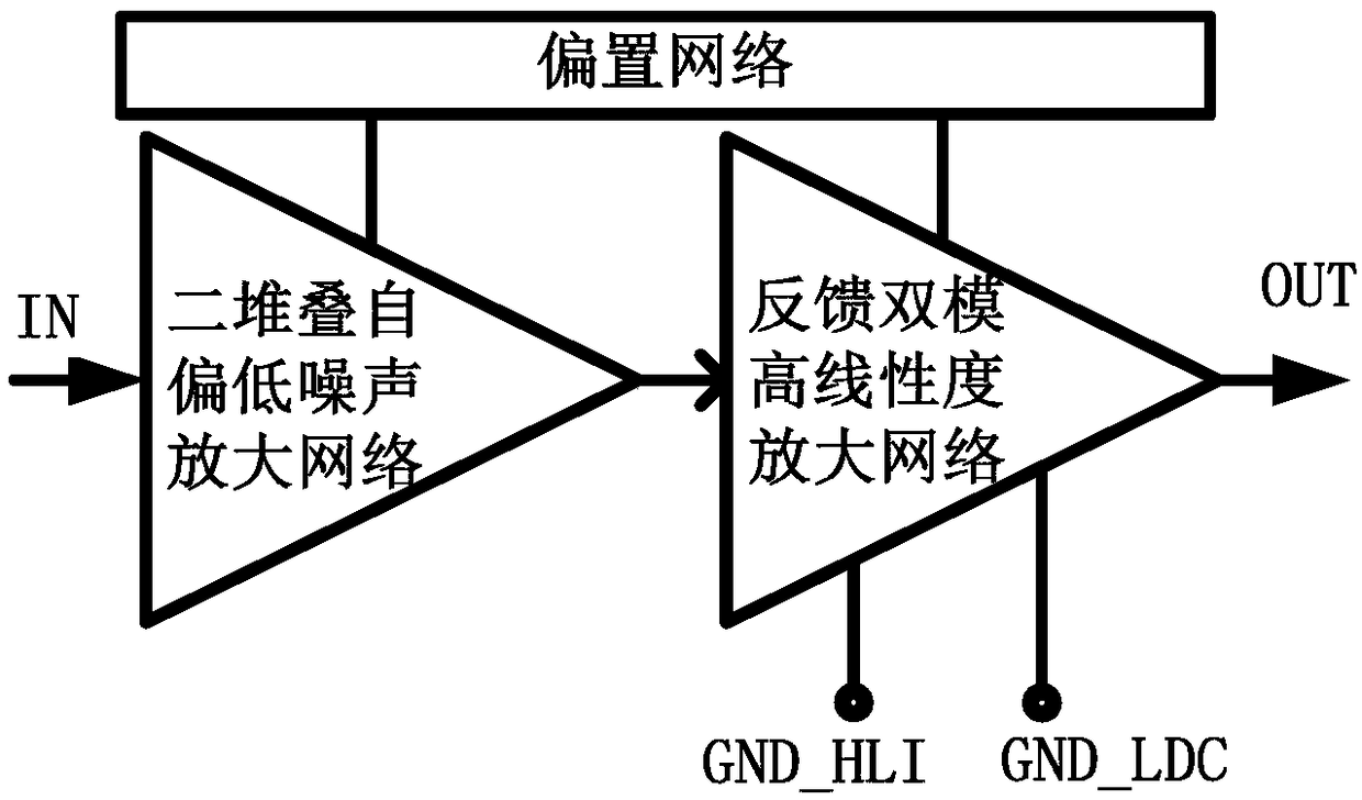
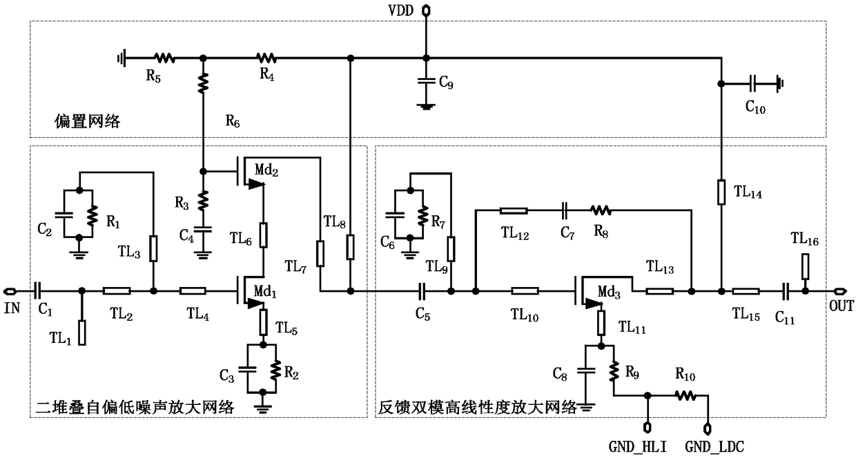
[0019] An embodiment of the present invention provides a low-power, high-linearity dual-mode millimeter-wave broadband stacked low-noise amplifier, such as figure 1As shown, it includes two stacked self-biased low-noise amplifier networks, feedback dual-mode high-linearity amplifier networks and bias networks; the input end of the two-stacked self-biased low-noise amplifier network is the input end of the entire low-noise amplifier, and its output end is the same as The input end of the feedback dual-mode high-linearity amplification network is connected; the output end of the feedback dual-mode high-linearity amplificat...


PUM


Abstract

The invention discloses a dual-mode millimeter wave broadband stacking low noise amplifier with low power consumption and high linearity. The dual-mode millimeter wave broadband stacking low noise amplifier comprises a two-stacking self-bias low noise amplification network, a feedback dual-mode high-linearity amplification network and a bias network. The dual-mode millimeter wave broadband stacking low noise amplifier disclosed by the invention adopts two transistors with different sizes to realize a serial stacking structure, and combines the self-bias technology to realize ultra-broadband noise matching, impedance matching and low power consumption; and meanwhile, a feedback dual-mode switching structure is adopted, so that the circuit has the switching capability in two modes, namely, high linearity and low power consumption, different usage requirements of users are met, and good broadband, gain and standing wave characteristics are obtained within the whole working frequency band.

Description

technical field [0001] The invention belongs to the technical field of field effect transistor radio frequency low noise amplifiers and integrated circuits, and in particular relates to the design of a low power consumption high linearity dual mode millimeter wave broadband stacked low noise amplifier. Background technique [0002] With the rapid development of military and civilian markets such as broadband communications and radar, RF front-end receivers are also developing in the direction of high performance, high integration, and low power consumption. Therefore, the market urgently needs ultra-wideband, high gain, high linearity, low Power consumption, low noise millimeter-wave low-noise amplifier chip, and the circuit supports switching capabilities in two modes with high linearity or low power consumption. [0003] However, in the design of traditional millimeter-wave low-noise amplifier chips, there have always been some design problems, mainly reflected in the mutu...

Claims


Application Information

Patent Timeline
Patent Type & Authority Applications(China)
IPC IPC(8): H03F3/193H03F3/68
CPCH03F3/193H03F3/68H03F2200/294H03F2200/451
Inventor 邬海峰滑育楠陈依军胡柳林吕继平童伟王测天
Owner CHENGDU GANIDE TECH
Learn More