Flexible cuprous oxide film, and preparation method and applications thereof
A cuprous oxide, thin film technology, applied in copper oxide/copper hydroxide, nanotechnology for materials and surface science, nanotechnology, etc.
- Summary
- Abstract
- Description
- Claims
- Application Information
AI Technical Summary
Problems solved by technology
Method used
Image
Examples
Embodiment 1
[0024] Embodiment 1 (film preparation method)
[0025] Deposit a 60 nm thick copper film on a pre-cleaned PET plastic substrate, immerse the copper film in a 1 mmol / L ammonium thiocyanate aqueous solution, react for 2 hours, and clean it with deionized water, that is, on the PET plastic substrate A cuprous thiocyanate film was formed on it. Immerse the cuprous thiocyanate film in 0.01 mol / liter sodium hydroxide aqueous solution, take it out after reacting for 1 hour, at this time the cuprous thiocyanate has completely transformed into a light yellow cuprous oxide film, rinse with deionized water, dry, That is, a cuprous oxide film is formed on a PET plastic substrate. Save for later.
[0026] The method of the invention can prepare a large-area thin film.
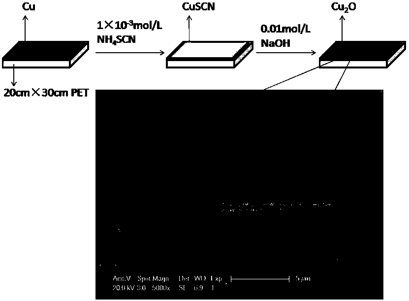
[0027] figure 1 The preparation of cuprous oxide thin films on plastic substrates is described.
[0028] SEM images show that the cuprous oxide film is composed of randomly distributed and uniform network nanowires. Mo...
Embodiment 2
[0031] Bending and half-folding tests on cuprous oxide film samples on PET plastic substrates:
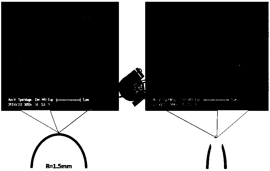
[0032] Sample 1: The film was repeatedly bent about 5,000 times with a bending radius of about 1.5 mm, and fixed into a curved shape (with a radius of curvature of about 1.5 mm), fixed on a small round table with double-sided adhesive tape for SEM observation.
[0033] Sample 2: Fold the film in half at 180°, flatten it with force to form creases, fix it on a small round table, and use SEM to observe the morphology and microstructure of the crease area.
[0034] figure 2 are schematic diagrams and typical SEM images of two samples. After the nanowire film is formed, the apparent thickness is much larger than that of the copper film, which can reach hundreds of nanometers.
[0035] Sample 1 (left) has undergone repeated bending, which is equivalent to repeated stretching and compression of the film (especially the nanowires on the upper surface) under the support of the substrate...
Embodiment 3
[0038] Corrosion resistance, organic solvent resistance, hot water resistance and other performance tests of cuprous oxide film samples:
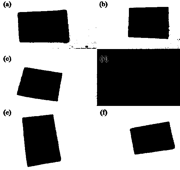
[0039] The cuprous oxide film samples (including plastic substrates) were placed in deionized water, 0.1 mol / liter sodium chloride solution, acetone, and N,N-dimethylformamide (DMF) for two months; The same sample was boiled in boiling water for 1 hour.
[0040] From the appearance, the film did not appear to fall off, such as image 3 shown. Soaking in acetone solution for a long time has some influence on the color of the film, which may be due to the photocatalytic performance of cuprous oxide, which changes the organic molecular structure and makes itself dyed; the color is somewhat uneven after boiling in boiling water for 1 hour, which may be due to high temperature In the lower atmospheric environment, some cuprous ions are oxidized to divalent cupric ions, and the hydrate of divalent cupric ions makes a small amount of blue-green ...
PUM
| Property | Measurement | Unit |
|---|---|---|
| Diameter | aaaaa | aaaaa |
| Elastic modulus | aaaaa | aaaaa |
| Hardness | aaaaa | aaaaa |
Abstract
Description
Claims
Application Information


