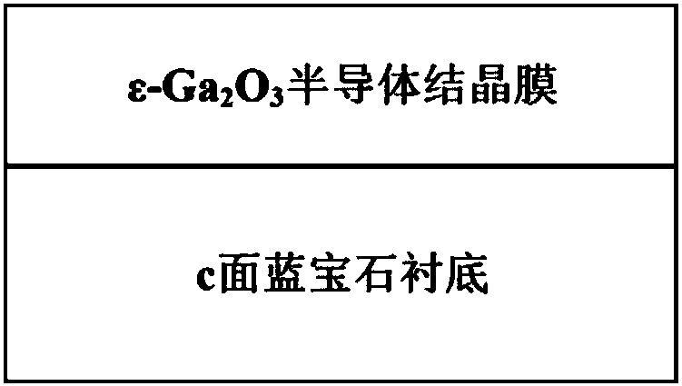
Laminated structure

A stacked structure, sapphire substrate technology, applied in coating, metal material coating process, gaseous chemical plating, etc., can solve the problems such as there is no ε-Ga2O3 thin film growth method

Active Publication Date: 2018-09-28
FUJIAN SUNWISE SEMICON TECH CO LTD
View PDF9 Cites 9 Cited by
  • Summary
  • Abstract
  • Description
  • Claims
  • Application Information

AI Technical Summary

Problems solved by technology

However, there is still no effective ε-Ga2O3 film growth method

Method used


Image

  • Laminated structure
  • Laminated structure
  • Laminated structure

Examples


Embodiment 1

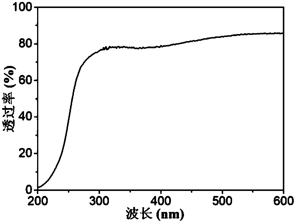
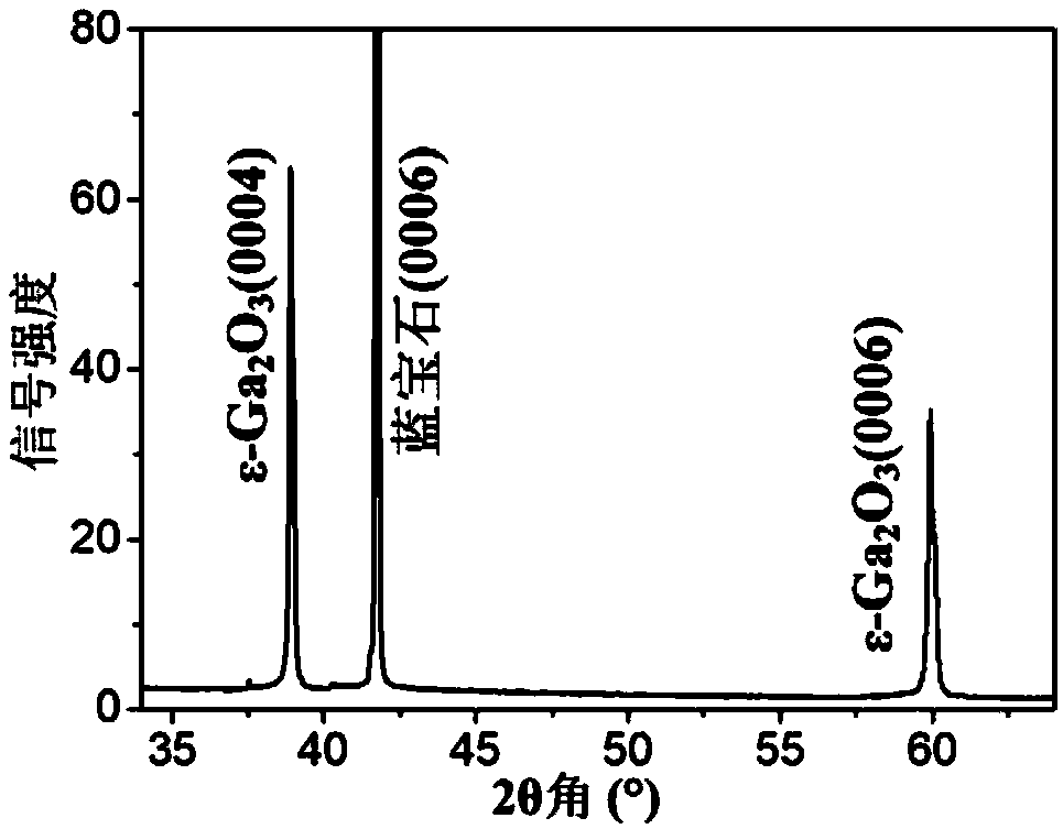
[0033] Metal-organic chemical vapor deposition (MOCVD) method to prepare high-quality ε-Ga 2 o 3 Layered structure of semiconductor crystal film.

[0034] Step 1: Select a clean sapphire substrate with a 0.2° deviation angle between the surface and the c-crystal plane and a thickness of 430 μm.

[0035] Step 2: The substrate is sent into the reaction chamber of the MOCVD equipment, and the tray is rotated at a speed of 750 rpm, ready for the epitaxial growth of the gallium oxide film.

[0036] Step 3: The temperature of the reaction chamber is raised to 550° C.; at the same time, 10 slm of supplementary argon gas is introduced into the reaction chamber, and the pressure of the reaction chamber is controlled at 80 Torr through the pressure control system.

[0037] Step 4: Immerse the bubble bottle filled with triethylgallium and deionized water in two constant temperature water tanks, control the temperature of the bubble bottle at 25°C and 25°C through the constant temperatu...

Embodiment 2

[0044] Preparation of high-quality tin-doped ε-Ga 2 o 3 Layered structure of semiconductor crystal film.

[0045] Step 1: Select a clean sapphire substrate with a 0° deviation angle between the surface and the c-crystal plane and a thickness of 100 μm.

[0046] Step 2: The substrate is sent into the reaction chamber of the MOCVD equipment, and the tray is rotated at a speed of 700 rpm, ready for the epitaxial growth of the gallium oxide film.

[0047] Step 3: The temperature of the reaction chamber is raised to 450° C.; at the same time, 8 slm of argon gas is introduced into the reaction chamber, and the pressure of the reaction chamber is controlled at 20 Torr through the pressure control system.

[0048] Step 4: Immerse the bubbling bottles filled with triethylgallium, deionized water, and tetrakis(dimethylamino)tin in three constant temperature water tanks, and control the temperature of the bubbling bottles to 25°C, 25°C, 2 ℃, and through mass flow meters and pressure g...

Embodiment 3

[0054] Prepare high quality ε-Ga 2 o 3 A stacked structure of a semiconductor PN junction.

[0055] Step 1: Select a clean sapphire substrate with a 10° off angle between the surface and the c crystal plane and a thickness of 1000 μm.

[0056] Step 2: The substrate is sent into the reaction chamber of the MOCVD equipment, and the tray is rotated at a speed of 900 rpm, ready for the epitaxial growth of the gallium oxide film.

[0057] Step 3: The temperature of the reaction chamber is raised to 800° C.; at the same time, 12 slm of argon gas is introduced into the reaction chamber, and the pressure of the reaction chamber is controlled at 400 Torr through the pressure control system.

[0058] Step 4: Immerse the bubbling bottles containing triethylgallium, deionized water, tetrakis(dimethylamino)tin, magnesocene, and ferrocene in five constant temperature water tanks, and control the temperature of the bubbling bottle by the constant temperature water tanks The temperature is...


PUM

PropertyMeasurementUnit
thicknessaaaaaaaaaa
thicknessaaaaaaaaaa
thicknessaaaaaaaaaa

Abstract

The invention provides a laminated structure capable of obtaining an epsilon-phase gallium oxide semiconductor crystal membrane and a corresponding preparation method. The laminated structure mainly comprises a sapphire substrate and the epsilon-phase gallium oxide semiconductor crystal membrane. The laminated structure is prepared in a manner of depositing the epsilon-phase gallium oxide semiconductor crystal membrane on the sapphire substrate by use of chemical vapor deposition. The sapphire substrate is 100 to 1,000 [mu]m thick. The real surface of the sapphire substrate forms a deviation angle of 0 to 10 degrees with the crystal face c of the sapphire substrate. The gallium oxide semiconductor crystal membrane is epsilon-phase gallium oxide with a hexagonal crystal system and is 0.1 to100 [mu]m thick. According to the laminated structure and the corresponding preparation method, the problem of difficulty in preparation of a pure-phase epsilon-Ga2O3 crystal membrane is solved and anovel technical way is provided for preparation of a gallium oxide semiconductor material.

Description

technical field [0001] The invention belongs to the field of semiconductor thin film materials, and mainly relates to a kind of ε-Ga with semiconductor function 2 o 3 Crystalline film stack structure. Background technique [0002] In applications such as large-scale transportation, electric energy, military radar, and spacecraft, etc., they are often faced with high-voltage and high-power working conditions; traditional Si materials have a small band gap (1.1eV) and a low critical breakdown electric field (0.3MV / cm ), so Si-based power electronic devices are difficult to apply to these occasions. The way to solve this problem is to use a new type of wide-bandgap semiconductor material to replace the traditional silicon material to make electronic devices. Ga 2 o 3 It has an ultra-wide band gap of 4.7-5.4eV, and the corresponding Baliga quality factor is much higher than that of currently commercialized Si (1.1eV), 4H-SiC (3.3eV) and GaN (3.4eV) and other materials. The...

Claims


Application Information

Patent Timeline
Patent Type & Authority Applications(China)
IPC IPC(8): H01L21/02H01L29/04H01L29/22C23C16/18C23C16/40
CPCC23C16/18C23C16/40H01L21/0242H01L21/02565H01L21/0262H01L29/04H01L29/22
Inventor 陈梓敏王钢李泽琦
Owner FUJIAN SUNWISE SEMICON TECH CO LTD
Why Eureka
Try Eureka