Partial intrinsic GaN cap layer RESURF (Reduced Surface Field) CaN-based Schottky barrier diode

A technology of Schottky potential and diode, applied in the direction of electrical components, circuits, semiconductor devices, etc., can solve the problems affecting the forward turn-on voltage and reverse withstand voltage of the device, difficult performance indicators, low diffusion coefficient, etc., reaching critical The effect of high breakdown electric field, excellent transient characteristics, and stable chemical properties

Inactive Publication Date: 2018-09-28
XIDIAN UNIV
View PDF4 Cites 4 Cited by
  • Summary
  • Abstract
  • Description
  • Claims
  • Application Information

AI Technical Summary

Problems solved by technology

For GaN materials, the diffusion coefficient of P-type impurities (such as Mg) in GaN is very low, so that accurate local doping cannot be achieved by thermal diffusion; and the ion implantation technology is not yet mature, and the lattice damage caused by it is difficult to use. annealing method to eliminate
[0004] To sum up, in traditional GaN-based Schottky barrier diodes, the Schottky contact barrier will affect the forward turn-on voltage and reverse withstand voltage of the device, and it is difficult to satisfy both at the same time to achieve high performance Index, which makes the device in the design and work, there is a compromise between forward loss and withstand voltage capability

Method used


Image

  • Partial intrinsic GaN cap layer RESURF (Reduced Surface Field) CaN-based Schottky barrier diode
  • Partial intrinsic GaN cap layer RESURF (Reduced Surface Field) CaN-based Schottky barrier diode
  • Partial intrinsic GaN cap layer RESURF (Reduced Surface Field) CaN-based Schottky barrier diode

Examples


Embodiment 1

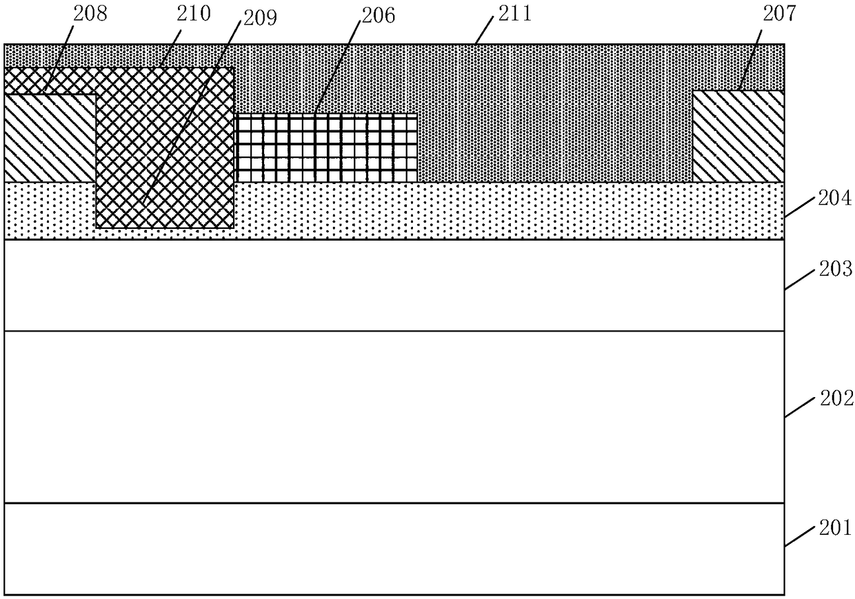
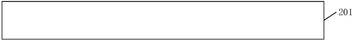
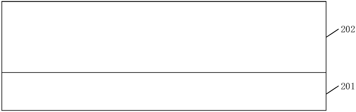
[0027] See figure 1 , figure 1 A schematic structural diagram of a partial intrinsic GaN cap layer RESURF GaN-based Schottky barrier diode provided for an embodiment of the present invention, including: a substrate layer 201, a buffer layer 202 on the substrate layer, and a buffer layer on the buffer layer A channel layer 203, a barrier layer 204 on the channel layer, a cathode and a composite anode at both ends of the barrier layer, a part of the intrinsic GaN cap layer connected to the composite anode and located on the barrier layer 206, covering the passivation layer 211 on the surface of the barrier layer 204, the part of the intrinsic GaN cap layer 206, the composite anode, and the cathode; the channel layer 203 is formed with the barrier layer 204 Heterojunction; the cathode is a cathode ohmic contact 207 , and the composite anode includes an anode ohmic contact 208 and an anode Schottky contact 210 .

[0028] The GaN-based Schottky barrier diode of the present invent...


PUM


Abstract

The invention relates to a partial intrinsic GaN cap layer RESURF (Reduced Surface Field) CaN-based Schottky barrier diode which comprises a substrate layer, a buffer layer, a channel layer 203, a barrier layer, a cathode and a composite anode, a partial intrinsic GaN cap layer and a passivation layer, wherein the buffer layer is positioned on the substrate layer; the channel layer is positioned on the buffer layer; the barrier layer is positioned on the channel layer; the cathode and the composite anode are positioned at both ends of the barrier layer; the partial intrinsic GaN cap layer is connected with the composite anode and positioned on the barrier layer; the passivation layer is covered on the barrier layer, the partial intrinsic GaN cap layer, the composite anode and the cathode;the channel layer and the barrier layer forms a heterojunction; the cathode is cathode ohmic contact; and the composite anode comprises an anode ohmic contact and an anode Schottky contact. Accordingto the embodiment of the invention, the partial intrinsic GaN cap layer is introduced on the barrier layer and the composite anode is adopted, so that the CaN-based Schottky barrier diode with a low forward turn-on voltage and a high reverse breakdown voltage is prepared.

Description

technical field [0001] The invention belongs to the field of semiconductors, and in particular relates to a partially intrinsic GaN cap layer RESURF GaN-based Schottky barrier diode. Background technique [0002] With the development of microelectronics technology, the performance of traditional first-generation Si semiconductors and second-generation GaAs semiconductor power devices has approached the theoretical limit determined by their materials themselves. Further reducing chip area, increasing operating frequency, reducing on-resistance, and improving breakdown voltage have become the focus of research at home and abroad. The wide bandgap semiconductor materials represented by gallium nitride (GaN) have stood out in the preparation of high-performance power devices in recent years, and their application potential is huge. GaN-based Schottky barrier diodes are ideal devices to replace Si-based Schottky barrier diodes. However, there are many deficiencies in current Ga...

Claims


Application Information

Patent Timeline
IPC IPC(8): H01L29/872H01L29/20
CPCH01L29/2003H01L29/872
Inventor 郑雪峰马晓华白丹丹王士辉吉鹏李纲董帅郝跃
Owner XIDIAN UNIV
Why Eureka
Try Eureka