
Sputtering target

A technology of sputtering target and target structure, applied in the field of sputtering target, which can solve the problems of unsteady sputtering, adhesion of conductive film, damage of transparent conductor layer, etc.

Inactive Publication Date: 2018-09-28
MITSUBISHI MATERIALS CORP
View PDF9 Cites 1 Cited by
  • Summary
  • Abstract
  • Description
  • Claims
  • Application Information

AI Technical Summary

Problems solved by technology

[0004] Here, in the above-mentioned conductive film, there is a problem that adjacent conductive films adhere to each other when wound into a roll, and damage occurs in the transparent conductor layer when the adhered conductive film is peeled off.
In a sputtering target with such a structure, the copper oxide phase whose conductivity is lower than that of metal Cu may cause abnormal discharge, and stable sputtering may not be performed.

Method used

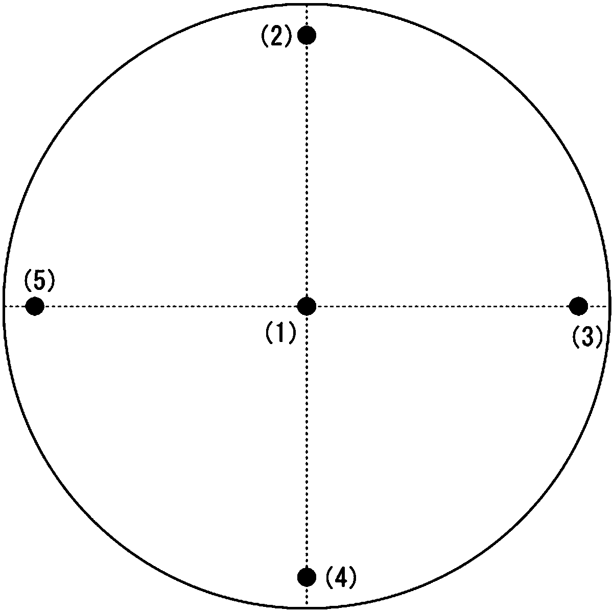
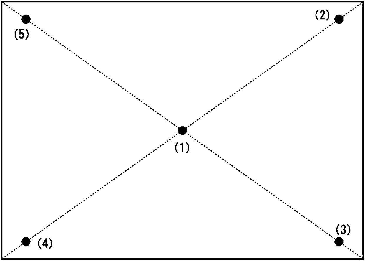
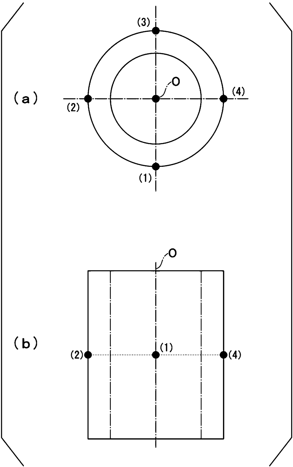

Image

  • Sputtering target
  • Sputtering target
  • Sputtering target

Examples


Embodiment

[0099] Hereinafter, the results of confirmation experiments conducted to confirm the effectiveness of the invention of the present application will be described.

[0100] (sputtering target)

[0101] As raw material powders, metallic copper powder (purity: 99.9% by mass or more, average particle size is shown in Table 1), CuO powder (purity: 99% by mass or more, average particle size: 5 μm), Cu 2 O powder (purity: 99% by mass or more, average particle diameter: 3 μm).

[0102] These raw materials were weighed so as to become the molar ratio recorded in Table 1, and in the container of the ball mill device set as the Ar gas atmosphere, the raw materials weighed and zirconia balls (diameter: 5mm), and mixed for 3 hours.

[0103] After sieving the obtained raw material powder, it is filled in a hot-pressed flat plate and cylindrical shape molding die, at 200kgf / cm 2 At the sintering temperatures shown in Table 1, the flat plate shape was maintained for 3 hours and the cylindri...


PUM

PropertyMeasurementUnit
Diameteraaaaaaaaaa

Abstract

This sputtering target is characterized by having a metal copper phase and an oxidized copper phase, wherein the volume fraction of the oxidized copper phase falls within a range of larger than 80 vol% but not larger than 90 vol%, the variation in specific resistance value at a target sputter surface is 50% or less with respect to the average specific resistance value, and the diameter of particles in the metal copper phase in the target structure falls within the range of 10-200 um. It is also preferable for the sputtering target to have the properties of a p-type semiconductor.

Description

technical field [0001] The present invention relates to a sputtering target used when forming a copper oxide film. [0002] This application claims the priority based on the patent application No. 2016-057461 filed in Japan on March 22, 2016 and the patent application No. 2017-038734 filed in Japan on March 1, 2017, and uses the contents thereof here. Background technique [0003] Generally, as a conductive film used in a touch sensor or the like, a conductive film having transparent conductive layers formed on both surfaces of the film and a metal layer formed on the surface of each transparent conductive layer is known. [0004] Here, the conductive film described above has a problem that adjacent conductive films adhere to each other when wound into a roll, and damage occurs in the transparent conductor layer when the adhered conductive film is peeled off. [0005] Therefore, Patent Document 1 proposes a film in which an inorganic nanocoat layer is formed on a film subst...

Claims


Application Information

Patent Timeline
IPC IPC(8): C23C14/34C04B35/45
CPCC04B35/45C23C14/3414
Inventor 斋藤淳井尾谦介盐野一郎张守斌
Owner MITSUBISHI MATERIALS CORP
Learn More