Semiconductor structure and formation method thereof

A technology of semiconductors and transistors, applied in the field of semiconductor structures and their formation, can solve the problems that the electrical properties of semiconductor structures need to be improved

Active Publication Date: 2018-10-09
SEMICON MFG INT (SHANGHAI) CORP +1
View PDF3 Cites 2 Cited by
  • Summary
  • Abstract
  • Description
  • Claims
  • Application Information

AI Technical Summary

Problems solved by technology

[0004] However, the electrical performance of prio

Method used


Image

  • Semiconductor structure and formation method thereof
  • Semiconductor structure and formation method thereof
  • Semiconductor structure and formation method thereof

Examples


Embodiment Construction

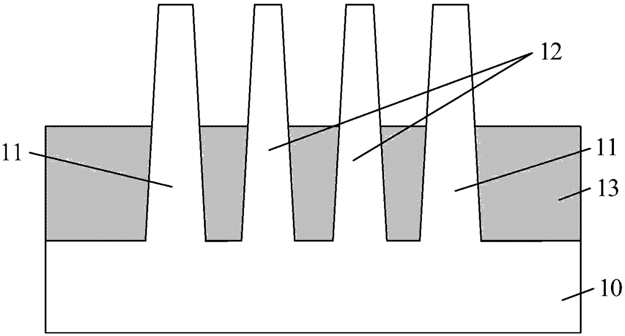
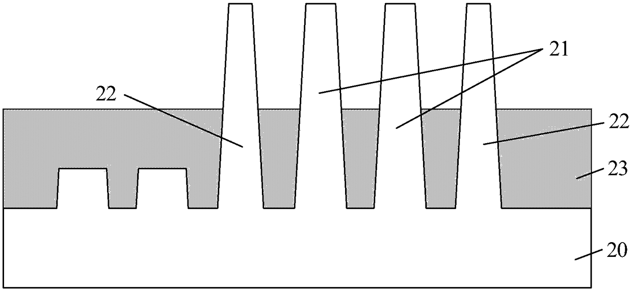
[0016] In order to improve the short channel effect, a common method is to perform an anti-punch through implant (Anti-punch Through Implant) process on the fin to form an anti-punch doping ion region in the fin. However, the electrical performance of the formed semiconductor structure still needs to be improved after introducing anti-punching ion implantation. Analyze the reasons for this:

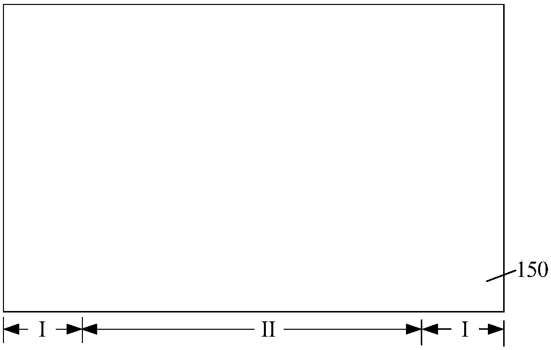
[0017] In semiconductor manufacturing, with the continuous reduction of feature size, in order to effectively fill the lithography gap of smaller nodes and improve the minimum pitch between adjacent semiconductor patterns, self-alignment process is more and more widely used. It is applied in fin formation process, such as self-aligned double patterned (Self-aligned Double Patterned, SADP) process. According to actual process requirements, the substrate includes a first region and a second region, the first region is used to form fin field effect transistors, and the second region is used...


PUM


Abstract

The invention provides a semiconductor structure and a formation method thereof. The method includes steps: providing a base comprising a first region used for forming a fin type field effect transistor and a second region used for forming an isolation structure; etching the base and forming a substrate and discrete fin portions located on the substrate of the first region, wherein the fin portions adjacent to the second region are first fin portions, the remaining fin portions are second fin portions, and the width dimensions of the first fin portions and the second fin portions are differentalong a direction parallel to the surface of the substrate and vertical to the extending direction of the fin portions; forming an isolating film on the substrate exposed by the fin portions, whereinthe isolating film covers sidewalls of the fin portions; performing an anti-punching through ion implantation process on the fin portion with the larger dimension in the first fin portions and the second fin portions after formation of the isolating film; and performing back-etching on a part thickness of the isolating film, and regarding the remaining isolating film as an isolation structure. According to the semiconductor structure and the formation method thereof, the short channel effect is improved, the carrier mobility of the semiconductor structure is increased, and the electrical performance of the formed semiconductor structure is enhanced.

Description

technical field [0001] The invention relates to the field of semiconductor manufacturing, in particular to a semiconductor structure and a forming method thereof. Background technique [0002] In semiconductor manufacturing, with the development trend of VLSI, the feature size of integrated circuits continues to decrease. In order to adapt to the reduction of feature size, the channel length of MOSFET field effect transistors is also continuously shortened accordingly. However, as the channel length of the device is shortened, the distance between the source and the drain of the device is also shortened, so the control ability of the gate to the channel becomes worse, and the gate voltage pinches off the channel. The difficulty is also increasing, making the phenomenon of subthreshold leakage (subthreshold leakage), the so-called short-channel effect (SCE: short-channel effects) more likely to occur. [0003] Therefore, in order to better adapt to the reduction of feature ...

Claims


Application Information

Patent Timeline
IPC IPC(8): H01L21/8234H01L27/088H01L29/78
CPCH01L21/823431H01L27/0886H01L29/785
Inventor 李勇
Owner SEMICON MFG INT (SHANGHAI) CORP
Why Eureka
Try Eureka