LED chip fabrication method

A technology of LED chip and manufacturing method, which is applied in semiconductor/solid-state device manufacturing, semiconductor devices, electrical components, etc., can solve the problems of easily damaged epitaxial layers, waste of resources, etc., and achieve light wavelength inconsistency, avoid damage, improve performance and quality effect

Active Publication Date: 2018-10-16
SOUTH UNIVERSITY OF SCIENCE AND TECHNOLOGY OF CHINA
View PDF12 Cites 3 Cited by
  • Summary
  • Abstract
  • Description
  • Claims
  • Application Information

AI Technical Summary

Problems solved by technology

[0006] The invention provides a method for manufacturing an LED chip to alleviate the problem of differences in LED chips caused by excessively large epitaxial wafers, and at the same time solve the problems of easy damage to the epitaxial layer during cutting and waste of resources caused during the transfer of LED chips

Method used


Image

  • LED chip fabrication method
  • LED chip fabrication method
  • LED chip fabrication method

Examples


Embodiment Construction

[0029] The present invention will be further described in detail below in conjunction with the accompanying drawings and embodiments. It should be understood that the specific embodiments described here are only used to explain the present invention, but not to limit the present invention. In addition, it should be noted that, for the convenience of description, only some structures related to the present invention are shown in the drawings but not all structures.

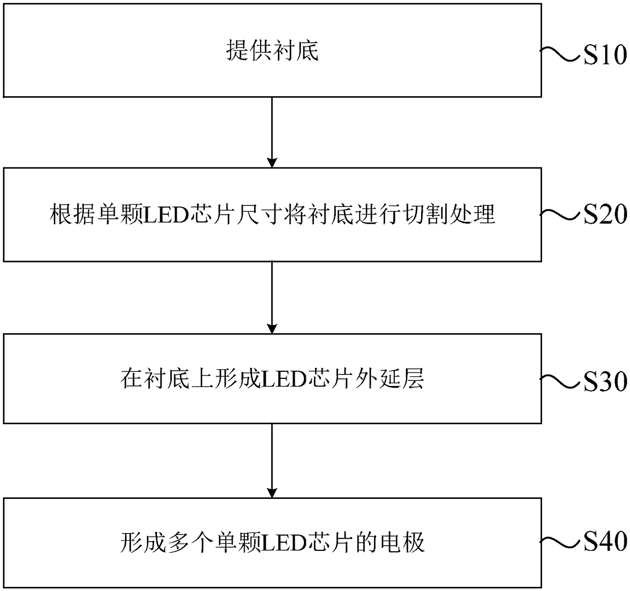
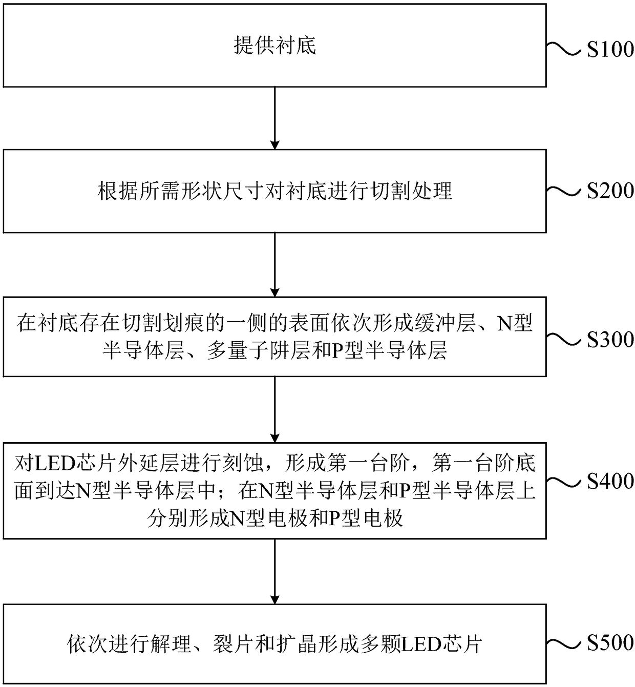
[0030] figure 1 It is a flow chart of a method for manufacturing an LED chip provided by an embodiment of the present invention. see figure 1 , the LED chip manufacturing method that the embodiment of the present invention proposes, comprises:

[0031] S10: providing a substrate.

[0032] In this embodiment, the material of the substrate is not limited, and the substrate may be a sapphire substrate, a silicon carbide substrate or other commonly used LED substrates.

[0033] S20: cutting the substrate according...


PUM


Abstract

The invention discloses an LED chip fabrication method. The LED chip fabrication method comprises the steps of providing a substrate; cutting the substrate according to a size of a single LED chip; forming an LED chip epitaxial layer on the substrate; and forming an electrode of a plurality of LED chips. According to the technical scheme provided by the invention, the substrate is cut, the LED chip epitaxial layer is formed on the cut substrate, damage to the epitaxial layer during the cutting process of the substrate can be prevented under the condition that an integral manufacturing processof the LED chips is not changed, the problems that light wavelength emitted from the formed LED chips caused by non-uniformity of the epitaxial layer and the problem of resource waste caused by transferring a large amount of LED chips can be effectively solved, the performance and the quality of the LED chips are improved, and time and resources are greatly saved.

Description

technical field [0001] Embodiments of the present invention relate to LED manufacturing technology, and in particular to a method for manufacturing an LED chip. Background technique [0002] Light Emitting Diode (LED) is a solid-state semiconductor electronic component that can emit light. Due to its high luminous efficiency, wide color range, and long service life, it is widely used in technical fields such as indicator lights, display screens, and lighting. [0003] In the traditional LED manufacturing method, the epitaxial layer is epitaxially grown on the substrate by metal organic compound chemical vapor deposition (Metal-organic Chemical Vapor Deposition, MOCVD) process, and then exposed electrodes are formed by evaporation and photolithography, and then cut to A plurality of single LED chips are obtained. However, the traditional LED manufacturing method is easy to damage the formed epitaxial layer in the process of cutting the slivers. [0004] In the development t...

Claims


Application Information

Patent Timeline
Patent Type & Authority Applications(China)
IPC IPC(8): H01L21/304H01L33/00
CPCH01L33/0066H01L21/3043
Inventor 孙小卫刘召军王立铎魏枫
Owner SOUTH UNIVERSITY OF SCIENCE AND TECHNOLOGY OF CHINA
Why Eureka
Try Eureka