

Air-coupled capacitive micromachining ultrasonic transducer, preparation method and application
A technology of capacitive micromachining and ultrasonic transducers, which is applied in chemical instruments and methods, vacuum evaporation plating, fluids using vibration, etc., can solve problems such as slow detection speed, achieve easy matching, low acoustic impedance, and achieve phase The effect of deflection control
- Summary
- Abstract
- Description
- Claims
- Application Information
AI Technical Summary
Problems solved by technology
Method used
Image

Examples
Embodiment 1
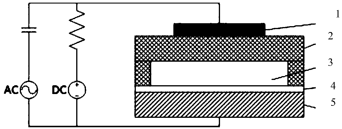
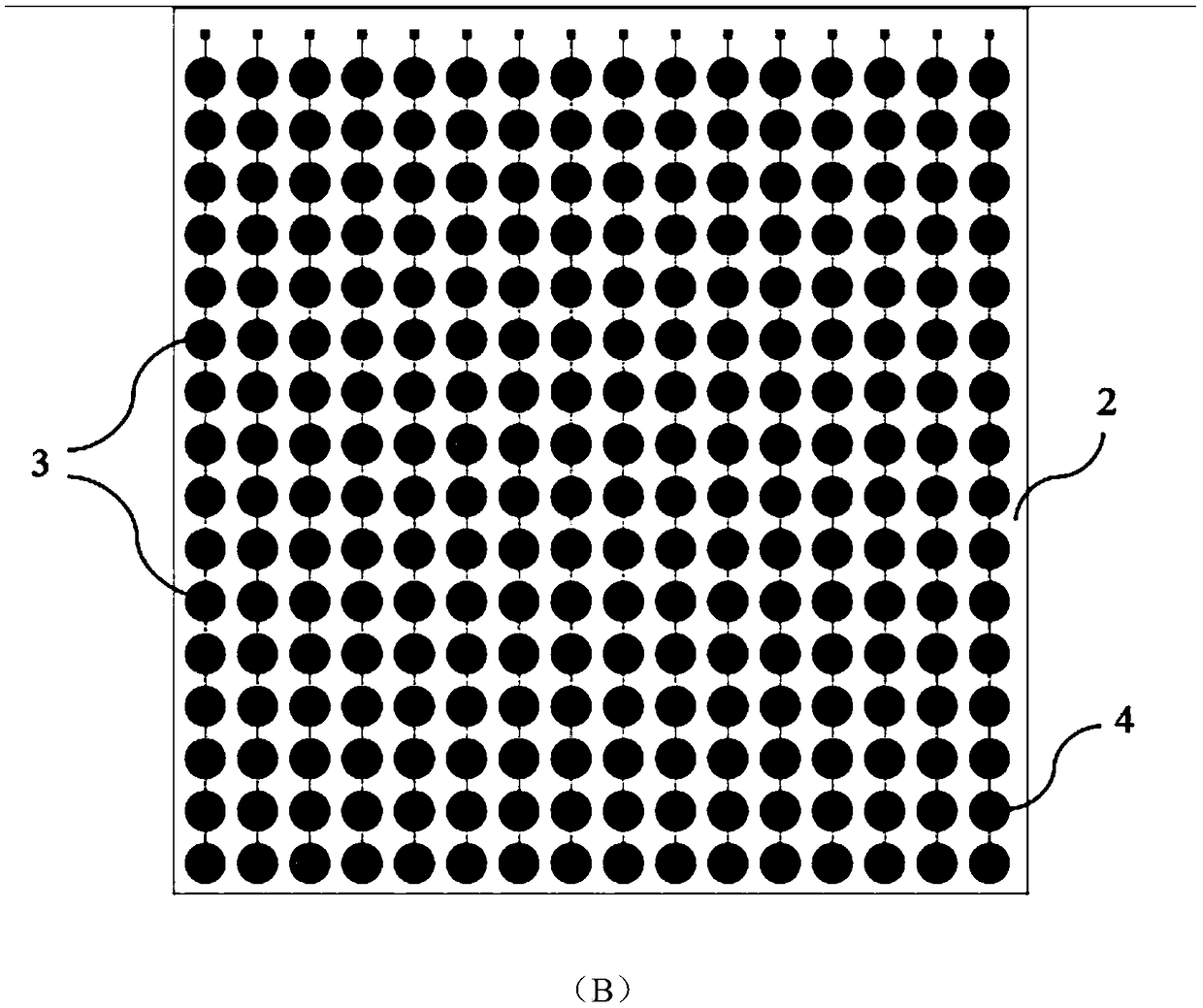
[0048] The purpose of the embodiment of the present invention is to provide a capacitive micro-ultrasonic transducer for ultrasonic nondestructive testing applied to air coupling. The transducer is composed of 16 array elements, and each array element is composed of multiple sensitive elements. See figure 2 (A).
[0049] The structure of each sensitive element is composed from top to bottom: upper electrode 3, diaphragm 1, cavity 5, and base 2 (wherein, base 2 is also used as the lower electrode), see figure 2 (B).
[0050] There is a cavity 5 between the diaphragm 1 and the base 2, which constitutes a capacitor, and a DC voltage is pre-loaded between the upper electrode 3 and the lower electrode 2, so that an electrostatic field is formed in the capacitor, and the diaphragm 1 under the action of the electric field force Deformation occurs under the diaphragm, thereby forming a pre-tightening force in the diaphragm 1, and the diaphragm 1 is in a stable equilibrium state.
...
Embodiment 2
[0054] Combine below figure 1 The scheme in Example 1 is further introduced, see the following description for details:
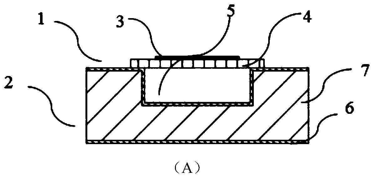
[0055] The overall structure of the embodiment of the present invention consists of two parts, the vibrating membrane 1 and the base 2 . The vibrating membrane 1 is composed of an upper electrode 3 and a thin film 4 .
[0056] In specific implementation, the thin film 4 may be a single crystal silicon thin film. It may also be set according to requirements in practical applications, which is not limited in this embodiment of the present invention.
[0057] Wherein, the material of the upper electrode 3 can be selected from gold, aluminum and the like. In the embodiment of the present invention, a single crystal silicon thin film is used as a component of the vibrating membrane 1 and the ultrasonic receiving sensitive element.
[0058] The base 2 is jointly formed by a cavity 5 and an insulating layer 6 . The material of the insulating layer 6 is silico...
Embodiment 3
[0061] see figure 2 (B), the embodiment of the present invention provides a preparation method of an air-coupled ultrasonic transducer, the preparation method is corresponding to the air-coupled ultrasonic transducer in Examples 1 and 2, and the preparation method includes:
[0062] The SOI wafer bonding technology adopted in the embodiment of the present invention is a bulk silicon process. This technology overcomes the defect of using a sacrificial layer, and processes a larger unit size through deep etching of the silicon base material, and has high processing reliability. The process flow of SOI wafer bonding process is as follows:
[0063] (A) Prepare silicon substrate 2, what silicon substrate 2 adopts is doped low-resistance silicon, thereby can form parallel plate capacitance with top electrode;
[0064] (B) Reactive ion etching (RIE) or wet etching is used to etch a cavity 5 with a target depth at a desired position, and the depth of the cavity 5 is 5 μm;
[0065]...
PUM
| Property | Measurement | Unit |
|---|---|---|
| Thickness | aaaaa | aaaaa |
| Thickness | aaaaa | aaaaa |
| Thickness | aaaaa | aaaaa |
Abstract
Description
Claims
Application Information