Double-sided capacitor structure and preparation method thereof

A capacitor structure and capacitor technology, applied in the manufacture of capacitors, electric solid devices, semiconductor/solid devices, etc., can solve the problems of short circuit, capacitance value reduction, capacitance area reduction, etc., and achieve the effect of dense density and increased capacitance area

Pending Publication Date: 2018-10-30
CHANGXIN MEMORY TECH INC
View PDF9 Cites 25 Cited by
  • Summary
  • Abstract
  • Description
  • Claims
  • Application Information

AI Technical Summary

Problems solved by technology

[0006] In view of the shortcomings of the prior art described above, the object of the present invention is to provide a double-sided capacitor structure and its preparation method, which is used to solve the problem that the opening area of ​​the capacitor hole is too large when removing the sacrificial layer in the prior art. Cause capacitor collapse and short circuit, the opening area of ​​the capacitor hole is too small and the sacrificial layer cannot be completely removed, resulting in the reduction of the capacitance area and the capacitance value

Method used


Image

  • Double-sided capacitor structure and preparation method thereof
  • Double-sided capacitor structure and preparation method thereof
  • Double-sided capacitor structure and preparation method thereof

Examples


Embodiment 1

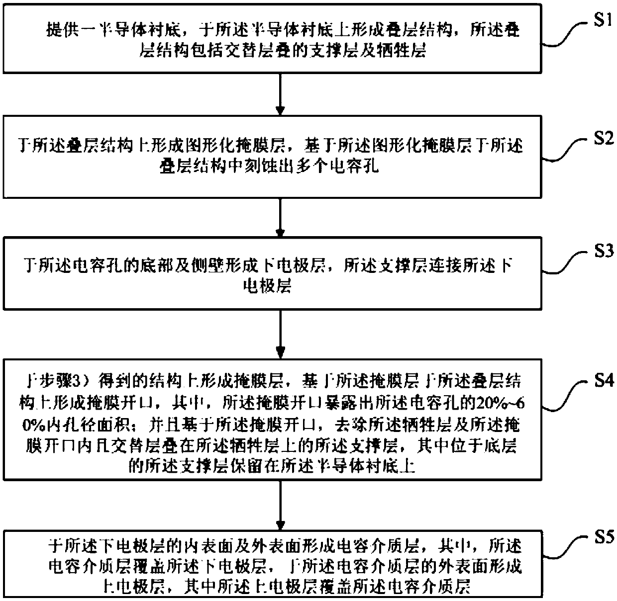
[0123] see figure 2 , the present embodiment provides a method for preparing a double-sided capacitor structure, the method for preparing a double-sided capacitor structure at least includes the following steps:

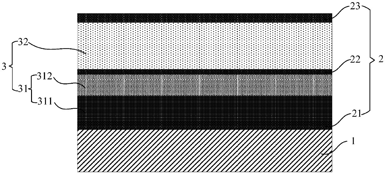
[0124] 1) A semiconductor substrate is provided, and a stacked structure is formed on the semiconductor substrate, the stacked structure comprising alternately stacked support layers and sacrificial layers;

[0125] 2) forming a patterned mask layer on the stacked structure, and etching a plurality of capacitance holes in the stacked structure based on the patterned mask layer;

[0126] 3) forming a lower electrode layer on the bottom and side walls of the capacitor hole, and the supporting layer is connected to the lower electrode layer;

[0127]4) Form a mask layer on the structure obtained in step 3), and form a mask opening on the stacked structure based on the mask layer, wherein the mask opening exposes 20% to 20% of the capacitor hole 60% of the inner apert...

Embodiment 2

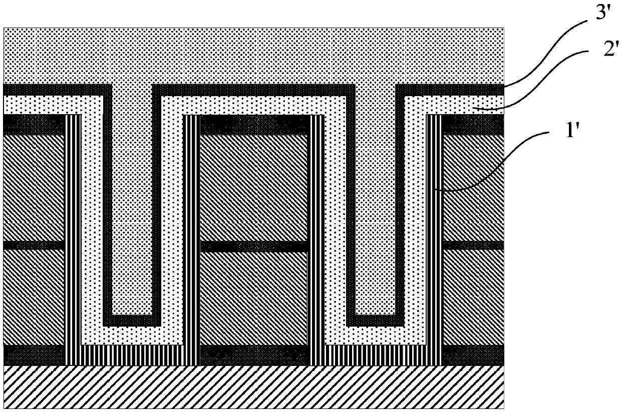
[0169] Please continue to refer to Embodiment 1 Figure 13 , the present invention also provides a double-sided capacitor structure, wherein the double-sided capacitor structure is preferably prepared by the preparation method of the present invention, of course, is not limited thereto, and the capacitor array structure includes:

[0170] semiconductor substrate 1;

[0171] The lower electrode layer 6 is formed on the semiconductor substrate 1, and the cross-sectional shape of the lower electrode layer 6 includes a U shape, wherein the height difference between the two sides of the U-shaped lower electrode layer 6 is 110 nm to 180 nm;

[0172] a capacitor dielectric layer 7 covering the inner and outer surfaces of the lower electrode layer 6;

[0173] The upper electrode layer 8 covers the outer surface of the capacitor dielectric layer 7 .

[0174] As an example, the semiconductor substrate 1 includes several capacitive contact nodes (not shown) in a memory array structure....


PUM


Abstract

The invention provides a preparation method of a double-sided capacitor structure. The preparation method of the double-sided capacitor structure comprises the following steps: 1) providing a semiconductor substrate, and forming a stacked structure on the semiconductor substrate; 2) forming a graphical mask layer on the stacked structure, and etching a plurality of capacitance holes in the stackedstructure based on the graphical mask layer; 3) forming a lower electrode layer at the bottom and side walls of the capacitance holes; 4) forming a mask layer on the structure obtained by the step 3,and forming a mask opening on the stacked structure based on the mask layer, wherein the opening exposes 20% to 60% inner aperture area of the capacitance holes; and removing a sacrificial layer based on the mask opening; and 5) forming a capacitive dielectric layer on the inner and outer surfaces of the lower electrode layer, and forming an upper electrode layer on the outer surface of the capacitive dielectric layer. The invention adopts different opening modes to form the double-sided capacitor with denser density, stronger mechanical strength and guaranteed capacitance value through controlling the opening area of the capacitor and using a supporting layer etching gas source.

Description

technical field [0001] The invention relates to the field of integrated circuit manufacturing, in particular to a double-sided capacitor structure and a preparation method thereof. Background technique [0002] Dynamic Random Access Memory (Dynamic Random Access Memory, DRAM) is a semiconductor memory device commonly used in computers, consisting of many repeated memory cells. Each memory cell usually includes a capacitor and a transistor; the gate of the transistor is connected to the word line, The drain is connected to the bit line, and the source is connected to the capacitor; the voltage signal on the word line can control the opening or closing of the transistor, and then read the data information stored in the capacitor through the bit line, or write the data information through the bit line stored in a capacitor. [0003] As the manufacturing process continues to evolve, the integration level of DRAM continues to increase, the size of components continues to shrink,...

Claims


Application Information

Patent Timeline
Patent Type & Authority Applications(China)
IPC IPC(8): H01L21/8242H01L27/108H01L23/64
CPCH01L28/92H10B12/30H10B12/03
Inventor 不公告发明人
Owner CHANGXIN MEMORY TECH INC
Why Eureka
Try Eureka