Method for controlling silicon single crystal growth temperature on basis of finite element numerical simulation

A technology of numerical simulation and growth temperature, applied in the direction of single crystal growth, single crystal growth, crystal growth, etc., can solve the problems of inability to meet crystal temperature control, crystal dislocation, etc.

Inactive Publication Date: 2018-11-06
XIAN UNIV OF TECH
View PDF8 Cites 11 Cited by
  • Summary
  • Abstract
  • Description
  • Claims
  • Application Information

AI Technical Summary

Problems solved by technology

[0003] The purpose of the present invention is to provide a silicon single crystal growth temperature control method based on finite element numerical simulation, which solves the problem that the silicon single crystal growth control method in the prior art cannot meet the crystal temperature control and cause crystal dislocation defects

Method used


Image

  • Method for controlling silicon single crystal growth temperature on basis of finite element numerical simulation
  • Method for controlling silicon single crystal growth temperature on basis of finite element numerical simulation
  • Method for controlling silicon single crystal growth temperature on basis of finite element numerical simulation

Examples


Embodiment Construction

[0068] The present invention will be described in detail below in conjunction with the accompanying drawings and specific embodiments.

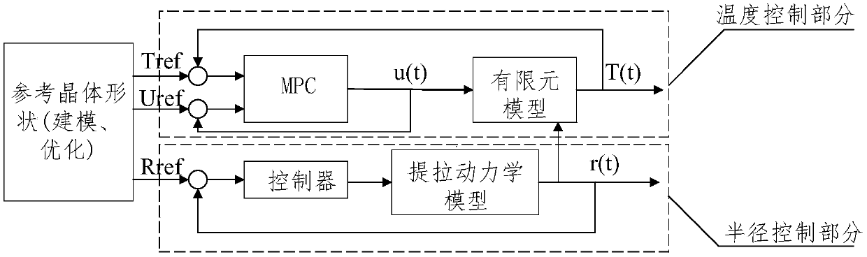
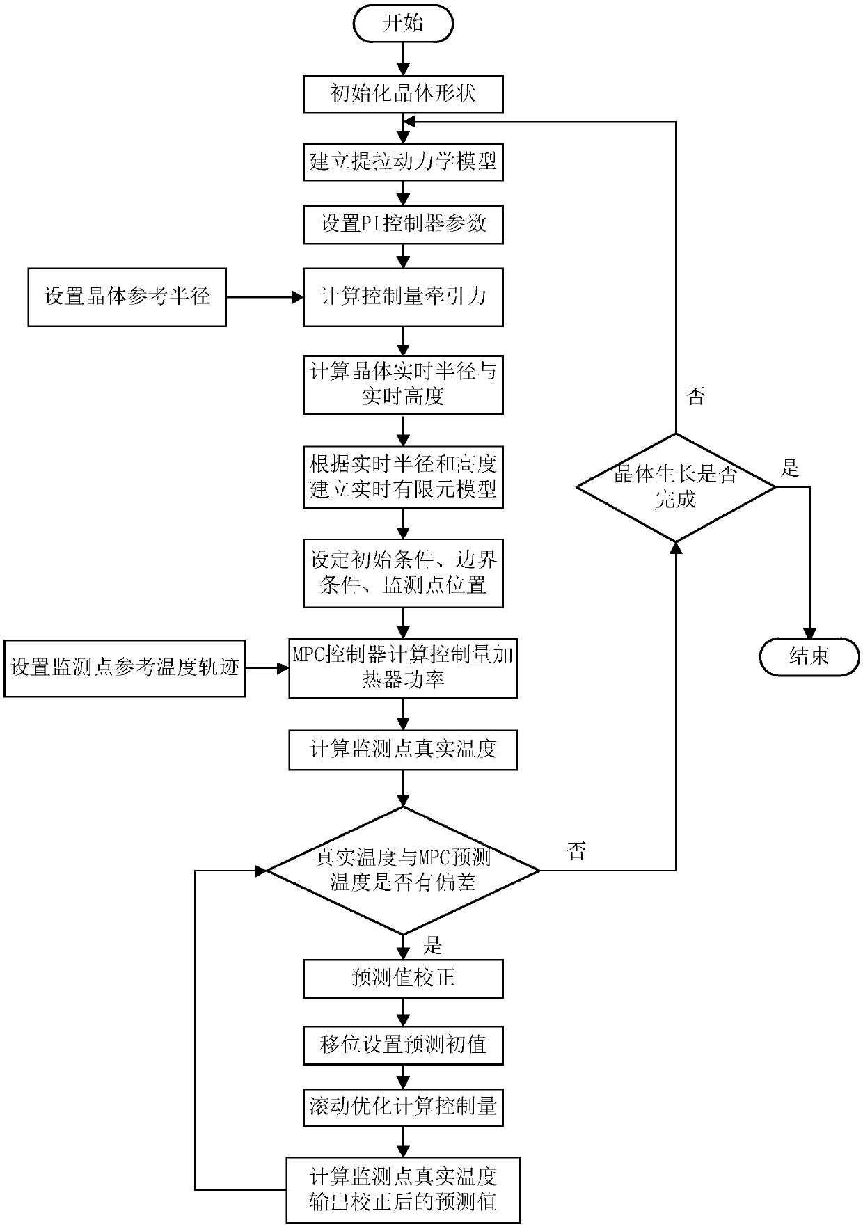
[0069] The present invention is a silicon single crystal growth temperature control method based on finite element numerical simulation. The crystal growth mainly includes four stages of shouldering, turning, equal diameter and finishing. The control block diagram is as follows figure 1 As shown, the specific steps are as follows:

[0070] Step 1. Refer to the finite element modeling under the crystal shape, and set the reference shape and boundary conditions of the crystal in the whole process. Specifically, follow the steps below:

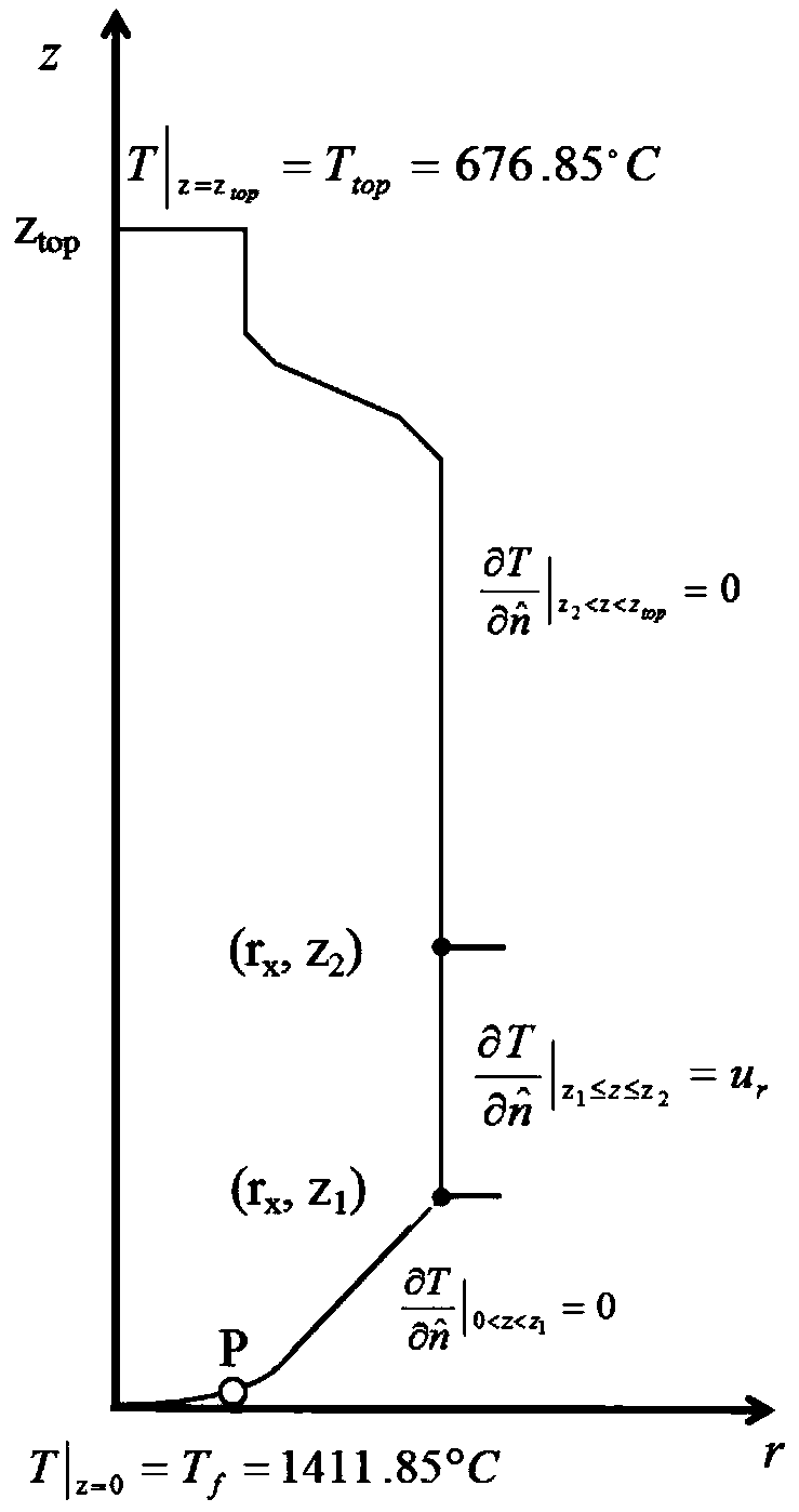
[0071] Step 1.1, the crystal heat conduction equation is as follows:

[0072]

[0073] In the formula Represents the spatial gradient in the cylindrical coordinate system, r represents the radius of the crystal, z represents the height of the crystal, T(r, z, t) represents the temperature at (r, z) in the ...


PUM


Abstract

The invention discloses a method for controlling silicon single crystal growth temperature on the basis of finite element numerical simulation. The method comprises the following steps: firstly, finite element modeling is performed by referring to crystal shape, and reference shape and boundary conditions of crystals in the whole process are set; the optimal trajectories, meeting constraints, of crystal temperature and heater power are calculated in an offline optimized manner with an optimization method by adopting the highest crystal cooling speed as the target and adopting adjustable rangeof the heater power and the maximum temperature gradient in the crystals as constraint conditions, and the optimal trajectories are used as reference input of a control system; then, crystal radius iscontrolled; finally, tracking control is performed on temperature trajectory in the crystals. The problem of crystal dislocation defect caused by the fact that crystal temperature control cannot be realized with the silicon single crystal growth control method in the prior art is solved.

Description

technical field [0001] The invention belongs to the technical field of temperature automatic control of Czochralski silicon single crystal growth process, and in particular relates to a silicon single crystal growth temperature control method based on finite element numerical simulation. Background technique [0002] Silicon single crystal is the most important semiconductor material. More than 90% of integrated circuit devices are fabricated on silicon single crystals. In recent years, with the rapid development of ultra-large-scale integrated circuit technology, the characteristic line width has been continuously reduced, and the requirements for the microscopic quality of crystals have become higher and higher. Dislocation is one of the important indicators to measure the quality of crystal, and temperature gradient and thermal stress are the main reasons for the formation of crystal dislocation defects. The origin of thermal stress lies in the temperature gradient insi...

Claims


Application Information

Patent Timeline
Patent Type & Authority Applications(China)
IPC IPC(8): C30B15/20C30B29/06
CPCC30B15/206C30B29/06
Inventor 刘丁张妮万银
Owner XIAN UNIV OF TECH
Why Eureka
Try Eureka