Field-effect transistor and its manufacturing method

A field-effect transistor and semiconductor technology, applied in semiconductor/solid-state device manufacturing, semiconductor devices, electrical components, etc., can solve the problems of affecting the performance of nano-scale devices, easy generation of epitaxial layers, and large contact resistance, etc., to reduce contact resistance, The effect of improving performance, improving quality and speed

Active Publication Date: 2017-09-22
CHINA RESOURCES MICROELECTRONICS (CHONGQING) CO LTD
View PDF1 Cites 0 Cited by
  • Summary
  • Abstract
  • Description
  • Claims
  • Application Information

AI Technical Summary

Problems solved by technology

[0005] In view of the above-mentioned shortcomings of the prior art, the purpose of the present invention is to provide a field effect transistor and its preparation method, which is used to solve the problem in the prior art that the in-situ doping and epitaxy of the source and drain regions rely on the sidewall of the far-floor extension region as a problem. Due to the epitaxial seed layer, defects are easily generated in the epitaxial layer, and the epitaxial speed is relatively slow, and due to the Salicide process without source and drain regions, the contact resistance of the contact hole and the source and drain regions is relatively large, which in turn affects nanoscale devices. performance problem

Method used


Image

  • Field-effect transistor and its manufacturing method
  • Field-effect transistor and its manufacturing method
  • Field-effect transistor and its manufacturing method

Examples


Embodiment 1

[0075] see Figure 1 to Figure 20 , one embodiment of the present invention provides a kind of preparation method of field effect transistor, the preparation method of described field effect transistor can be suitable for the preparation of quasi-SOI source-drain High K Metal Gate last gate process MOSFET, at least comprises the following steps:

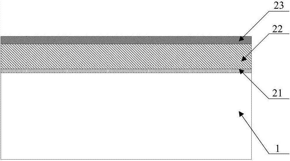
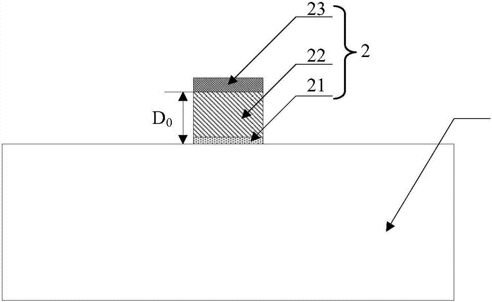
[0076] 1) Provide a semiconductor substrate 1, and form a first gate stack structure 2 on the semiconductor substrate 1; wherein, in the illustrated embodiment, the gate stack structure 2 is a dummy gate, from bottom to top sequentially comprising a gate oxide layer 21, a polysilicon layer 22 and a gate hard mask layer 23;

[0077] 2) forming first spacers 31 on both sides of the first gate stack structure 2;

[0078] 3) forming a recessed structure 4 outside the first sidewall 31; forming an insulating dielectric layer 41 in the recessed structure 4;

[0079] 4) performing in-situ doping epitaxy, forming a source-drain structure 6...

Embodiment 2

[0117] see Figure 21 to Figure 23 , Another embodiment of the present invention provides a kind of preparation method of field effect transistor, the preparation method of described field effect transistor can be suitable for the preparation of quasi-SOI source-drain High K Metal Gate front gate process MOSFET, at least comprises the following steps:

[0118] 1) A semiconductor substrate 1 is provided, and a first gate stack structure 2 is formed on the semiconductor substrate 1 by a gate-front process; wherein in the illustrated embodiment, the first gate stack structure 2 is true Gate, including an oxide interface layer 24, a high dielectric constant layer 25, a work function adjustment layer 26 and a metal gate layer 27 from bottom to top;

[0119] 2) forming first spacers 31 on both sides of the first gate stack structure 2;

[0120] 3) forming a recessed structure 4 outside the first sidewall 31; forming an insulating dielectric layer 41 in the recessed structure 4;

...

Embodiment 3

[0136] see Figure 24 to Figure 26 Another embodiment of the present invention also provides a method for preparing a field effect transistor, which is suitable for the preparation of a quasi-SOI source-drain conventional gate MOSFET, and at least includes the following steps:

[0137] 1) A semiconductor substrate 1 is provided, and a first stacked gate structure 2 is formed on the semiconductor substrate 1 by a conventional process, and the first stacked gate structure 2 includes a gate oxide layer 21, polysilicon layer 22 and gate hard mask layer 23;

[0138] 2) forming first spacers 31 on both sides of the first gate stack structure 2;

[0139] 3) forming a recessed structure 4 outside the first sidewall 31; forming an insulating dielectric layer 41 in the recessed structure 4;

[0140] 4) performing in-situ doping epitaxy, forming a source-drain structure 61 above the insulating dielectric layer 41, and using the semiconductor substrate 1 outside the recessed structure 4...


PUM


Abstract

The invention provides a field effect transistor and a preparation method thereof. The method comprises the steps of: providing a semiconductor substrate, forming a first gate stack structure on the semiconductor substrate, and forming first side walls on two sides of the first gate stack structure; forming a recessed structure in the semiconductor substrate outside the first side walls; forming an insulating dielectric layer in the recessed structure; performing in-situ doping, forming a drain-source structure on the insulating dielectric layer; and forming an isolation structure on the semiconductor substrate outside the drain-source structure. By using a post-isolation process, when a drain-source area is doped and extended in-site, the semiconductor substrate outside the drain-source area is taken as an epitaxy seed crystal layer, and the epitaxy quality and speed are greatly improved.

Description

technical field [0001] The invention belongs to the technical field of ultra-large-scale integrated circuit manufacturing, and relates to a field-effect transistor and a preparation method thereof. Background technique [0002] For planar MOSFETs, when the channel length shrinks, the short channel effect will become more and more serious. For the advanced FDSOI (Full Depletion Semiconductor on Insulation) substrate material, the short channel effect can be effectively controlled, but SOI has its own shortcomings, mainly self heating effect (Self Heating Effect) and floating body effect (Floating Body Effect), These effects will affect the performance of SOI devices, and in severe cases will cause device failure. Therefore, how to improve the self-heating effect and floating body effect of SOI devices has become a research hotspot in the industry. Among them, a MOSFET device called quasi-SOI can well avoid self-heating effect and floating body effect. Since the channel regi...

Claims


Application Information

Patent Timeline
Patent Type & Authority Patents(China)
IPC IPC(8): H01L21/335H01L29/772
CPCH01L29/0847H01L29/665H01L29/66553H01L29/78
Inventor 黄晓橹
Owner CHINA RESOURCES MICROELECTRONICS (CHONGQING) CO LTD
Why Eureka
Try Eureka