Crucible for quasi-monocrystalline silicon ingot casting and taking silica film as barrier layer

A technology of quasi-single crystal silicon and silicon dioxide, which is applied in the field of crucibles for quasi-single crystal silicon ingots, can solve the problems of increasing the cost of ingots, the limited effect of the width of the red zone at the bottom of the silicon ingots, etc., so as to improve the utilization rate and structure. Dense and uniform effect

Inactive Publication Date: 2018-11-06
ZHEJIANG UNIV
View PDF10 Cites 1 Cited by
  • Summary
  • Abstract
  • Description
  • Claims
  • Application Information

AI Technical Summary

Problems solved by technology

However, the effect of reducing the width of the red zone at the bottom of the silicon ingot is relatively limited, and the use of high-purity materials increases the cost of ingot casting

Method used


Image

  • Crucible for quasi-monocrystalline silicon ingot casting and taking silica film as barrier layer
  • Crucible for quasi-monocrystalline silicon ingot casting and taking silica film as barrier layer
  • Crucible for quasi-monocrystalline silicon ingot casting and taking silica film as barrier layer

Examples


Embodiment 1

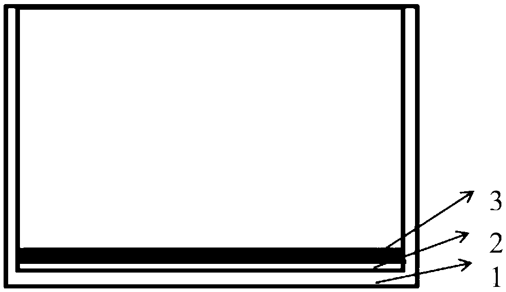
[0028] (1) Provide an inner diameter of 175*175mm and a crucible with a height of 190mm, spray a layer of silicon nitride coating on the inner surface of the base of the crucible, and let it dry naturally;

[0029] (2) Provide a solar-grade monocrystalline silicon wafer with a thickness of 0.2mm and a specification of 170*170mm;

[0030] (3) Anneal at 900°C for 15 minutes by thermal oxidation method on the above-mentioned solar-grade monocrystalline silicon wafer, grow silicon dioxide on both sides, and paste it on the inner bottom of the crucible through high-purity silica sol;

[0031] The SiO 2 The thickness of the film is 10nm;

[0032] (4) Then, a seed crystal is set on the barrier layer at the bottom of the crucible, and silicon material is set on the seed crystal, followed by heating, melting, crystal growth, annealing, and cooling to obtain a quasi-single crystal silicon ingot.

[0033] The schematic diagram of the silicon nitride coating, barrier layer, seed crystal...

Embodiment 2

[0037] (1) Provide an inner diameter of 175*175mm and a crucible with a height of 190mm, spray a layer of silicon nitride coating on the inner surface of the base of the crucible, and let it dry naturally;

[0038] (2) Provide a solar-grade monocrystalline silicon wafer with a thickness of 0.2mm and a specification of 170*170mm;

[0039] (3) Anneal at 900°C for 30 minutes by thermal oxidation method on the above-mentioned solar-grade monocrystalline silicon wafer, grow silicon dioxide on both sides, and paste it on the inner bottom of the crucible through high-purity silica sol;

[0040] The SiO 2 The thickness of the film is 15nm;

[0041] (4) Then, a seed crystal is set on the barrier layer at the bottom of the crucible, and silicon material is set on the seed crystal, followed by heating, melting, crystal growth, annealing, and cooling to obtain a quasi-single crystal silicon ingot.

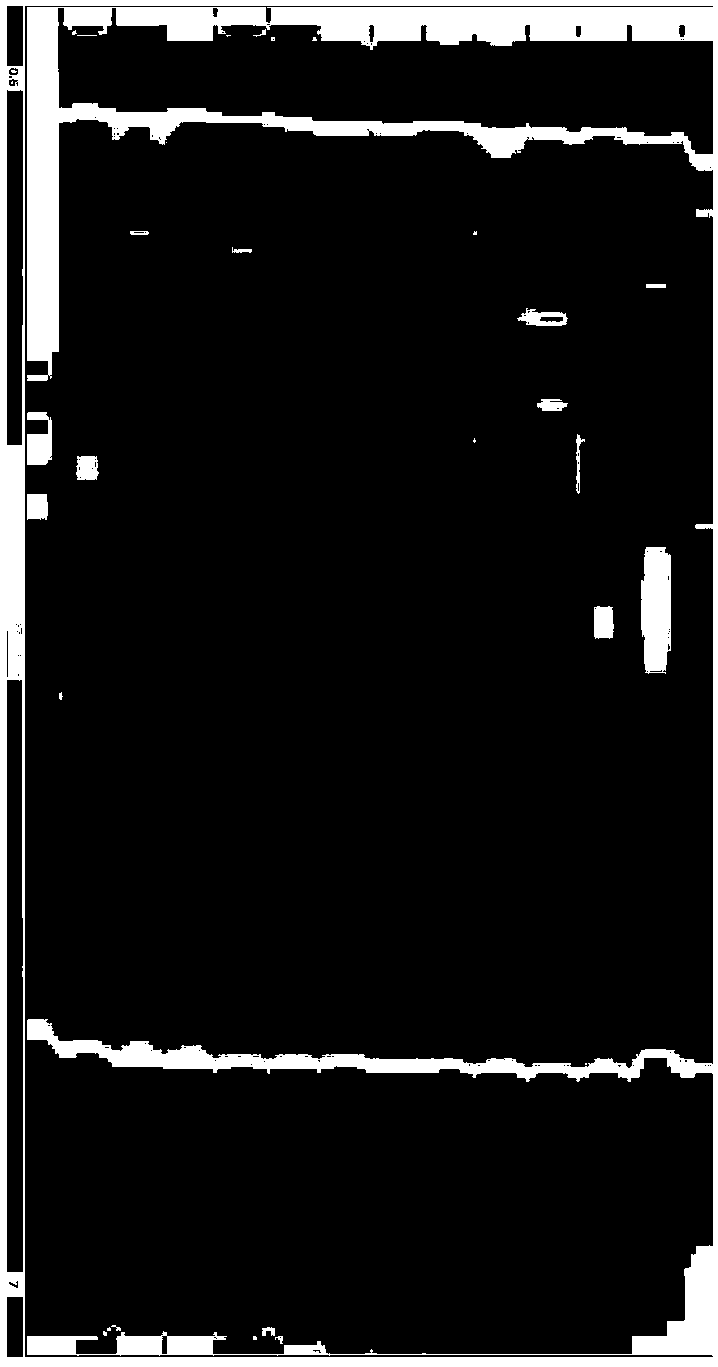
[0042] The minority carrier lifetime in the bottom region of the quasi-single crystal si...

Embodiment 3

[0044] (1) Provide an inner diameter of 175*175mm and a crucible with a height of 190mm, spray a layer of silicon nitride coating on the inner surface of the base of the crucible, and let it dry naturally;

[0045] (2) Provide a solar-grade monocrystalline silicon wafer with a thickness of 0.2mm and a specification of 170*170mm;

[0046] (3) Anneal at 1000°C for 30 minutes by thermal oxidation method on the above-mentioned solar-grade monocrystalline silicon wafer, grow silicon dioxide on both sides, and paste it on the inner bottom of the crucible through high-purity silica sol;

[0047] The SiO 2 The thickness of the film is 30nm;

[0048] (4) Then set the seed crystal on the bottom barrier layer in the crucible, and then set the silicon material on the seed crystal, after heating, melting, crystal growth, annealing, and cooling to obtain a 160*160*128mm quasi-single crystal silicon ingot .

[0049] The minority carrier lifetime diagram of the quasi-single crystal silicon...


PUM

PropertyMeasurementUnit
thicknessaaaaaaaaaa
heightaaaaaaaaaa
thicknessaaaaaaaaaa

Abstract

The invention discloses a crucible for quasi-monocrystalline silicon ingot casting and taking a silica film as a barrier layer. The inner surface of the base of the crucible is provided with a siliconnitride coating and a barrier layer. The barrier layer is a solar energy level monocrystalline silicon substrate, and a SiO2 film grows on the substrate through a thermal oxidation method. The red area width of the bottom of a quasi-monocrystalline silicon ingot, which is prepared through the provided crucible, is about 4 mm; the minority carrier lifetime of the ingot is greater than 2 [mu]s, andthe utilization rate of the quasi-monocrystalline silicon ingot is improved effectively. The provided quasi-monocrystalline silicon ingot can be cut into silicon chips, the impurity concentration ofsilicon chips is low, the minority carrier lifetime of silicon chips is long; the efficiency of batteries prepared from the silicon chips is high, and the average conversion efficiency is 18-18.5%.

Description

technical field [0001] The invention belongs to the field of quasi-single crystal silicon ingots, and in particular relates to a crucible for quasi-single crystal silicon ingots using a silicon dioxide film as a barrier layer. Background technique [0002] As a renewable clean energy, solar energy has been widely used in grid-connected power generation, civil Power generation, public facilities and integrated energy-saving buildings. In the field of solar power generation, crystalline silicon photovoltaic power generation systems occupy a major position in the new energy photovoltaic power generation market. The market has increasingly stringent requirements on the quality of mono / polysilicon, the raw material that affects photovoltaic power generation. [0003] In the current quasi-single crystal casting / polycrystalline casting process, impurities in the crucible such as iron, oxygen, carbon, etc. will diffuse into the silicon ingot at high temperature, and metal impuriti...

Claims


Application Information

Patent Timeline
Patent Type & Authority Applications(China)
IPC IPC(8): C30B35/00C30B29/06
CPCC30B35/002C30B29/06
Inventor 余学功胡泽晨杨德仁
Owner ZHEJIANG UNIV
Why Eureka
Try Eureka