Broadband filter based on artificial local surface plasmons
A local surface plasmon and filter technology, applied to waveguide devices, electrical components, circuits, etc., can solve the problems of difficult compression length, unfavorable circuit miniaturization design, slenderness, etc., and achieve good group delay and well-balanced Effect of shape, compact circuit area
- Summary
- Abstract
- Description
- Claims
- Application Information
AI Technical Summary
Problems solved by technology
Method used
Image
Examples
Embodiment 1
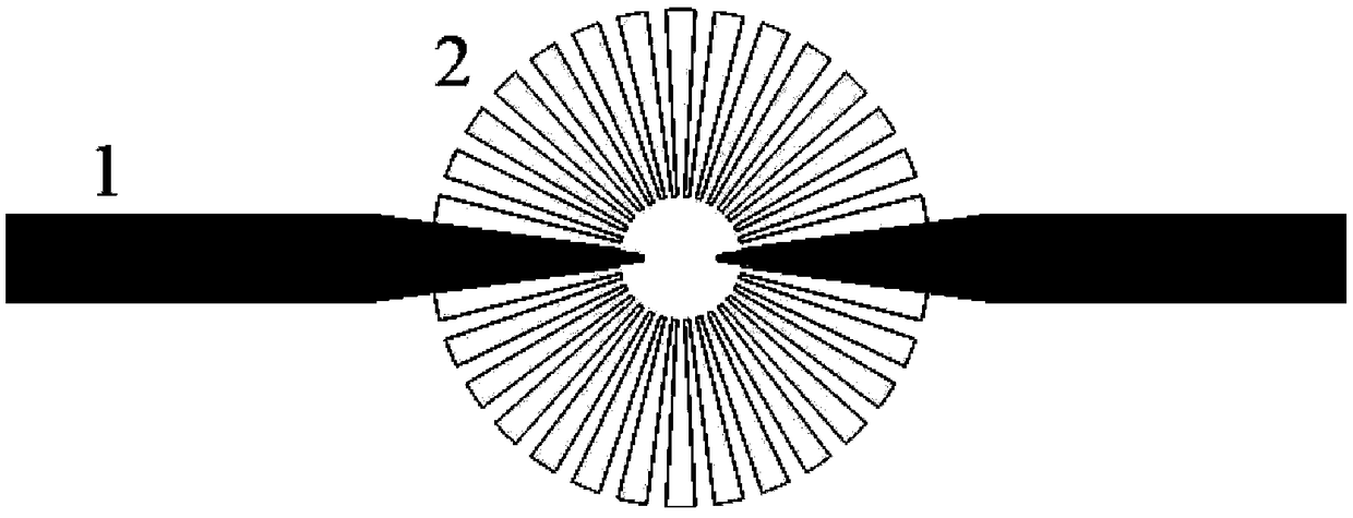
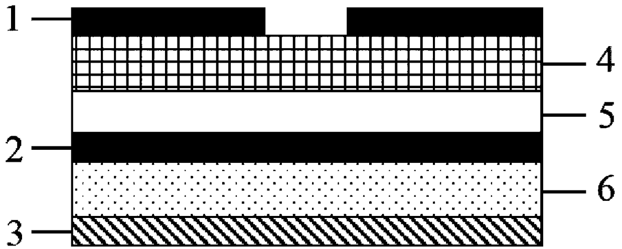
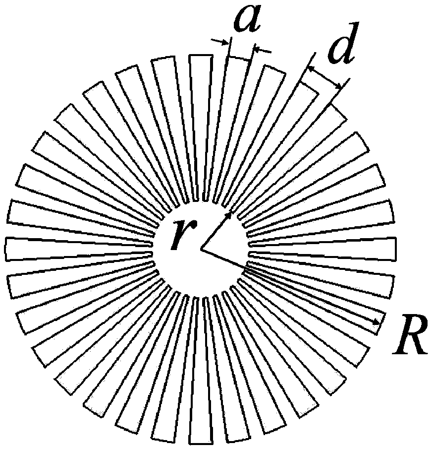
[0035] Embodiment 1 of the present invention, the structure is as Figure 1-4 As shown, the upper dielectric substrate 4 and the lower dielectric substrate 6 are both 0.508mm thick Rogers RT5880 (prepreg) with a dielectric constant of 3.5, a dielectric loss angle of 0.004, and a thickness of 0.1mm. The microstrip excitation structure 1, the artificial localized surface plasmon 2 and the large-area metal ground 3 are all copper with a thickness of 0.018 mm. The parameters of the artificial localized surface plasmon structure in this embodiment are: r=2.5mm, R=10mm, N=32, a / d=0.6, that is, a=0.82mm, d=1.96mm; the microstrip excitation structure The parameter is: w 1 = 3.5mm, w 2 =0.2mm, l=12.5mm, s=3mm.
[0036] The simulation and test S parameter of embodiment one are as Figure 5 shown. The band-pass filter in the present embodiment, center frequency 4.3GHz, 3dB bandwidth 53% (3dB bandwidth is defined as S21 >-3dB corresponds to the frequency bandwidth divided by the cent...
Embodiment 2
[0038] In the second embodiment of the present invention, the materials and material thicknesses used are the same as those in the first embodiment. Among them, the structural parameters of artificial localized surface plasmons are: r=2.5mm, R=5mm, N=32, a / d=0.6; the structural parameters of microstrip excitation are: w 1 = 3.5mm, w 2 =0.2mm, l=7.5mm, s=2mm.
[0039] The simulation of embodiment two and test S parameter such as Figure 6 shown. The center frequency of the bandpass filter in this embodiment is 11.7GHz, and the 3dB bandwidth is 73%. (Tested S 21 The data is lower than the simulated value at high frequency, because the SMA connector used in the test has a low operating frequency and a large loss above 10GHz. ) The group delay in the passband of this filter is 1ns, and the initial edge of the parasitic passband is at 31GHz (about 3.6 times the center frequency).
PUM
| Property | Measurement | Unit |
|---|---|---|
| Thickness | aaaaa | aaaaa |
| Thickness | aaaaa | aaaaa |
| Thickness | aaaaa | aaaaa |
Abstract
Description
Claims
Application Information


