Manufacturing method of transistor gate

A manufacturing method and transistor technology, applied in the fields of semiconductor/solid-state device manufacturing, semiconductor devices, electrical components, etc., can solve the problems of poor roughness of the critical dimension of transistor gates, affecting transistor characteristics, etc., to improve characteristics, eliminate influence, and eliminate The effect of differences in gate critical dimensions

Active Publication Date: 2020-11-24
SHANGHAI HUALI INTEGRATED CIRCUIT CORP
View PDF5 Cites 0 Cited by
  • Summary
  • Abstract
  • Description
  • Claims
  • Application Information

AI Technical Summary

Problems solved by technology

like Figure 3a and 3b shown in Figure 2f On the basis of the gate cutting and polysilicon etching, the gate morphology is obtained. The critical dimension of the final gate has a large difference between the active region and the isolation region, and the roughness of the critical dimension of the entire transistor gate is poor. thus affecting the characteristics of the transistor

Method used


Image

  • Manufacturing method of transistor gate
  • Manufacturing method of transistor gate
  • Manufacturing method of transistor gate

Examples


Embodiment Construction

[0024] The technical solutions in the present invention will be clearly and completely described below in conjunction with the accompanying drawings. Apparently, the described embodiments are part of the embodiments of the present invention, not all of them. Based on the embodiments of the present invention, all other embodiments obtained by persons of ordinary skill in the art without making creative efforts belong to the protection scope of the present invention.

[0025] In an embodiment of the present invention, a method for manufacturing a gate of a transistor is provided. Specifically, the manufacturing method of the transistor gate includes the following steps:

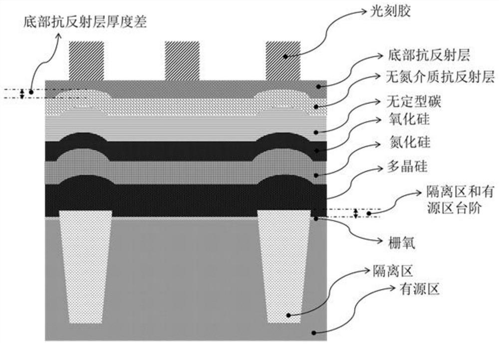
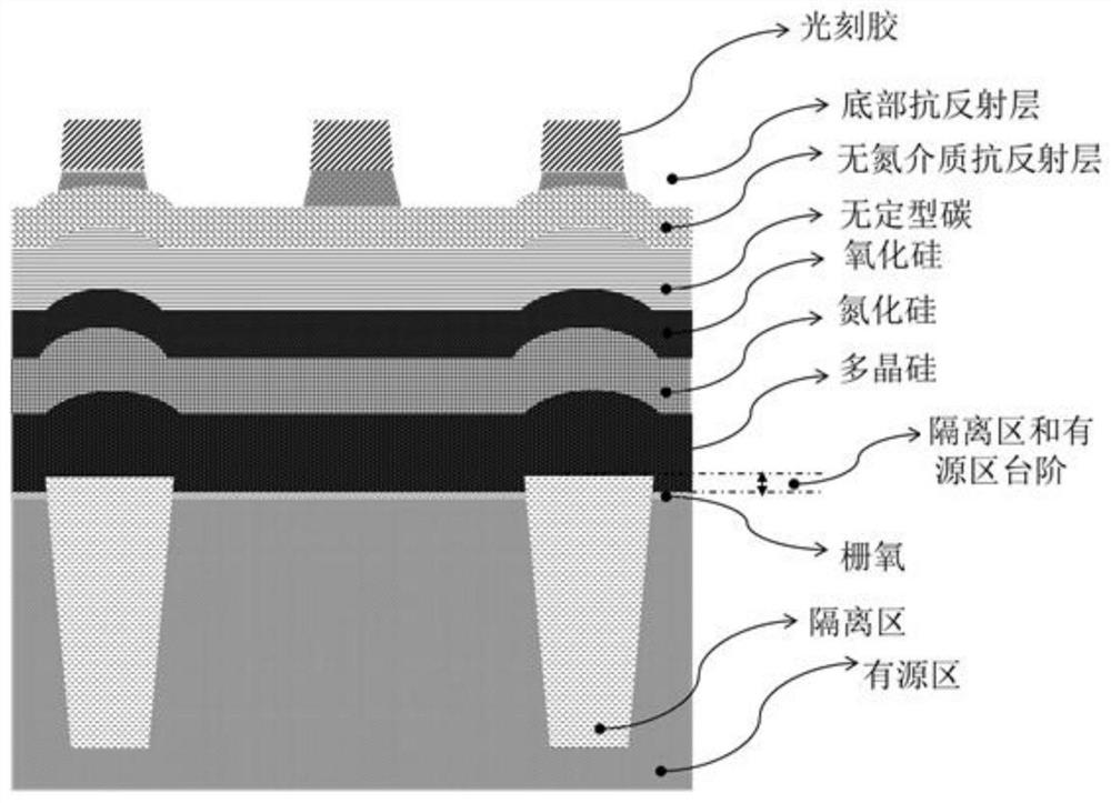
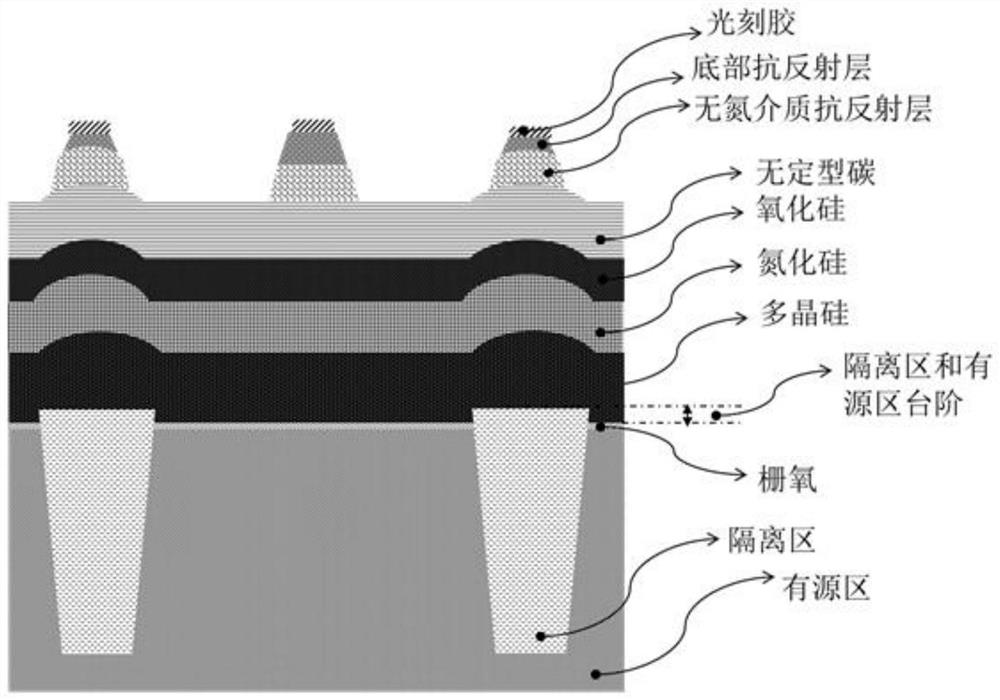
[0026] In step S1, polysilicon, silicon nitride, silicon oxide, an amorphous carbon layer (APF) and an organic coating material layer are sequentially deposited on the isolation region and the active region.

[0027] Specifically, see Figure 4a , Figure 4a It is a schematic diagram of the manufacturing pro...


PUM


Abstract

The invention relates to a manufacturing method of a transistor grid, and relates to a manufacturing technology of an integrated circuit. The manufacturing method comprises the steps of sequentially depositing upper poly-silicon, silicon nitride, silicon oxide, an amorphous carbon layer and an organic coating material layer on an isolation region and an active region; etching the organic coating material layer, and further eliminating bulges on a surface of the amorphous carbon layer so that the surface of the amorphous carbon layer after an etching process is smooth; depositing a nitrogen-free dielectric anti-reflection layer, coating a bottom anti-reflection layer, and performing a photoresist coating developing process; sequentially performing etching of the bottom anti-reflection layerand etching of the nitrogen-free dielectric anti-reflection layer, amorphous carbon, a silicon oxide film and a silicon nitride film; removing the amorphous carbon; and cutting a grid of a transistor, and etching the poly-silicon to obtain grid morphology of the transistor so that the influence of the bottom anti-reflection layer on a key size of the transistor grid is eliminated and the characteristic of the transistor is improved.

Description

technical field [0001] The invention relates to an integrated circuit manufacturing technology, in particular to a method for manufacturing a gate of a transistor. Background technique [0002] In the manufacture of semiconductor integrated circuits, the critical dimensions of transistor gates are an important measure of the level of integrated circuit manufacturing and design. [0003] The gate critical dimension is mainly determined by the hard mask etching process (especially below the 28nm process node). In the hard mask etching process, polysilicon, silicon nitride, silicon oxide, amorphous carbon, and nitrogen-free dielectric anti-reflective layer are deposited sequentially on the isolation region and the active region through a deposition process, and then the bottom layer is coated. Anti-reflection layer, photoresist. Specifically, refer to figure 1 , figure 1 It is a schematic diagram of the manufacturing process of a transistor in the prior art. Such as figur...

Claims


Application Information

Patent Timeline
Patent Type & Authority Patents(China)
IPC IPC(8): H01L21/28H01L21/027
CPCH01L21/0276H01L29/401
Inventor 陆连朱轶铮
Owner SHANGHAI HUALI INTEGRATED CIRCUIT CORP
Why Eureka
Try Eureka