A silicon carbide mosfet device and manufacturing method thereof

A silicon carbide and device technology, applied in semiconductor devices, electrical components, circuits, etc., can solve problems such as high power loss, high production cost, and poor robustness

Active Publication Date: 2021-01-08
UNIV OF ELECTRONICS SCI & TECH OF CHINA
View PDF10 Cites 0 Cited by
  • Summary
  • Abstract
  • Description
  • Claims
  • Application Information

AI Technical Summary

Problems solved by technology

[0007] The present invention needs to be solved, that is, aiming at the above-mentioned problems, it is proposed to propose a method that can optimize the poor robustness, high power loss, and poor workability caused by the excessive electric field of the gate dielectric layer in the application of silicon carbide MOSFET devices such as inverter circuits and chopper circuits. Silicon carbide MOSFET device with low efficiency, high production cost and other problems and its manufacturing method

Method used


Image

  • A silicon carbide mosfet device and manufacturing method thereof
  • A silicon carbide mosfet device and manufacturing method thereof
  • A silicon carbide mosfet device and manufacturing method thereof

Examples


Embodiment 1

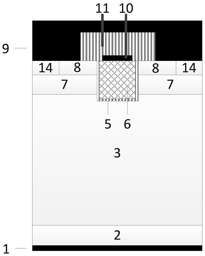
[0074] A silicon carbide MOSFET device such as figure 2 As shown, the cellular structure includes a drain metal 1, a silicon carbide N+ substrate 2 and a silicon carbide N- epitaxial layer 3 arranged in sequence from bottom to top; the silicon carbide N- epitaxial layer 3 has a source trench above it, so The source trench is filled by deposition of Schottky contact metal 12 or polysilicon 13, and the Schottky contact metal 12 or polysilicon 13 is in direct contact with the silicon carbide N-epitaxial layer 3 to form a Schottky contact or Si / SiC heterojunction contact; the left and right sides of the Schottky contact metal 12 on the semiconductor surface are respectively embedded with a silicon carbide deep P-doped region 4, and the depth of the two silicon carbide deep P-doped regions 4 is deeper than that of the Schottky The bottom of the base contact metal 12, the upper left of the silicon carbide deep P-doped region 4 on the left side of the Schottky contact metal 12, and ...

Embodiment 2

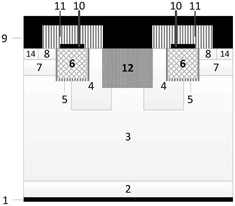
[0076] Such as image 3 As shown, this embodiment is roughly the same as Embodiment 1, except that the structure does not have a silicon carbide P+ contact region 14, but on the upper left of the silicon carbide N- epitaxial layer 3, the silicon carbide Pbase region 7 and the carbide The left side of the silicon N+ source region 8 has a silicon carbide deep P-doped region 4 , and the silicon carbide deep P-doped region 4 has the same depth as the silicon carbide deep P-doped region 4 near the gate structure. This improvement helps to strengthen the protection of the silicon carbide deep P-doped region 4 on the semiconductor surface structure, so that the long-term application reliability of the device is improved.

Embodiment 3

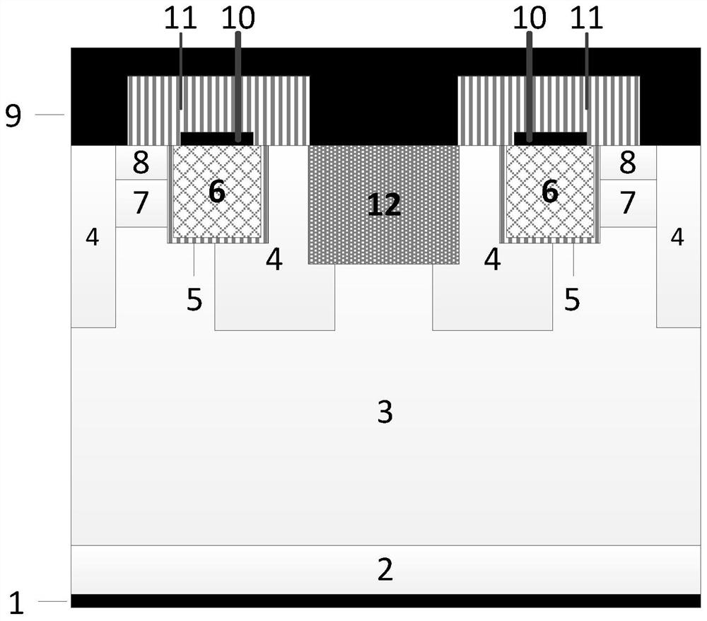
[0078] The structure of this embodiment is substantially the same as that of Embodiment 1, except that the Schottky contact metal 12 region used is replaced by polysilicon 13, as Figure 4 shown. Also, a Si / SiC heterojunction structure with a rectifying contact is formed on the bottom sidewall of the source trench and the silicon carbide N- epitaxial layer 3 . The forward conduction voltage drop Von of the heterojunction structure is about 1.1V, which also has a good effect on improving the operation of the third quadrant of the device. At the same time, since the heterojunction is a multi-sub-device, the diode has good reverse recovery performance.


PUM

PropertyMeasurementUnit
thicknessaaaaaaaaaa
widthaaaaaaaaaa
widthaaaaaaaaaa

Abstract

The invention provides a silicon carbide MOSFET device and a manufacturing method thereof. The invention forms a discontinuous gate structure on the basis of a common silicon carbide UMOSFET structure, and introduces two silicon carbide deep P gate structures between the two gate structures. Implantation region, while introducing metal or polysilicon between two silicon carbide deep P implantation regions. The metal or polysilicon is in direct contact with the SiC N-epitaxy to form a Schottky contact or a heterojunction contact with rectification characteristics. This improvement greatly optimizes the basic characteristics of the traditional SiC UMOSFET and realizes a multi-sub rectifier device The integration of the device greatly optimizes the working performance of the third quadrant of the device, and at the same time, the invention has the characteristics of low Miller capacitance, simple process and easy realization.

Description

technical field [0001] The invention belongs to power semiconductor technology, in particular, relates to a metal oxide semiconductor field effect (MOSFET) device structure and a manufacturing method thereof. Background technique [0002] The development and efficient utilization of energy resources is an eternal theme of human development. Since human history entered the 21st century, the world's energy production and consumption are still dominated by fossil energy. Combined with the current development and utilization of energy resources, fossil energy will still be the energy basis for human survival and development in a relatively long period of time. However, fossil energy will eventually be exhausted, and it is easy to cause environmental pollution problems. The resulting environmental and sustainable development problems are difficult problems that human beings must face. Electric energy is one of the main forms of energy available to human beings, and improving it...

Claims


Application Information

Patent Timeline
Patent Type & Authority Patents(China)
IPC IPC(8): H01L29/06H01L29/16H01L29/66H01L29/78
CPCH01L29/0603H01L29/1608H01L29/66477H01L29/78
Inventor 张金平邹华赵阳罗君轶李泽宏张波
Owner UNIV OF ELECTRONICS SCI & TECH OF CHINA
Why Eureka
Try Eureka