Passivation contact electrode structure and applicable solar cell and manufacturing method thereof

A solar cell and contact electrode technology, applied in circuits, photovoltaic power generation, electrical components, etc., can solve the problems of increasing carrier Auger recombination loss, difficulty in mass production, irradiation loss, etc., and reduce surface recombination efficiency. , strong electrical conductivity, the effect of reducing radiation loss

Pending Publication Date: 2018-11-13
SUZHOU SUNWELL NEW ENERGY CO LTD
View PDF0 Cites 25 Cited by
  • Summary
  • Abstract
  • Description
  • Claims
  • Application Information

AI Technical Summary

Problems solved by technology

However, the currently used laboratory metallization processes such as physical vapor deposition and evaporation on the surface passivation contact structure are difficult to apply to mass production, while the use of screen printing and firing throu

Method used


Image

  • Passivation contact electrode structure and applicable solar cell and manufacturing method thereof
  • Passivation contact electrode structure and applicable solar cell and manufacturing method thereof
  • Passivation contact electrode structure and applicable solar cell and manufacturing method thereof

Examples


Embodiment 1

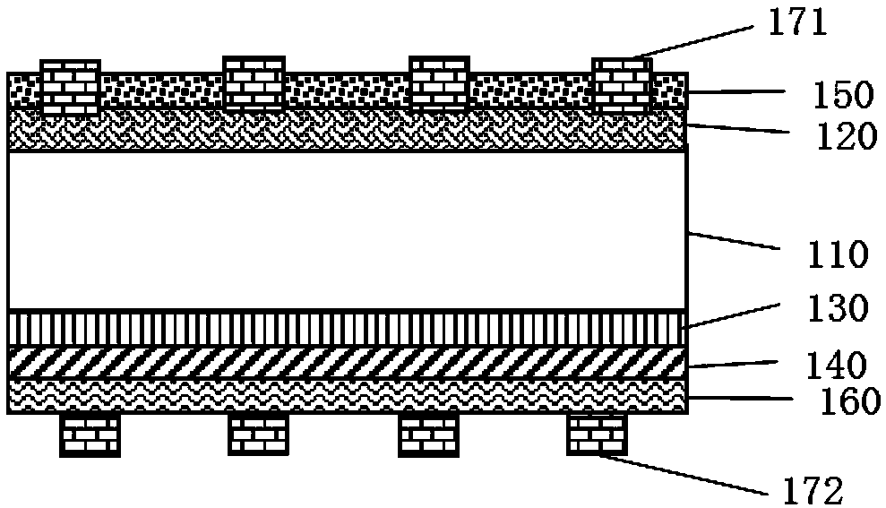
[0034] figure 1 An exemplary diagram illustrating fabrication of a solar cell according to an embodiment of the present invention is illustrated.

[0035] The crystalline silicon substrate 110 may be an n-type or p-type crystalline silicon wafer with a thickness of 70-250 μm. In this embodiment, the crystalline silicon substrate 110 is preferably a p-type crystalline silicon wafer, which may be a single crystal or polycrystalline silicon wafer. The p-type crystalline silicon substrate 110 is cleaned and textured. Phosphorus is diffused on the front side of the textured p-type crystalline silicon substrate to form an n-type doped crystalline silicon layer 120 emitter.

[0036] Fabricate passivated contact electrode structures on the back of the cell. The passivation contact electrode structure includes a doped semiconductor layer 140 deposited on the crystalline silicon substrate 110 as one of doped polysilicon, microcrystalline silicon or microcrystalline silicon-carbon all...

Embodiment 2

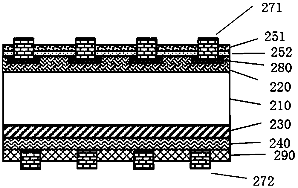
[0045] figure 2 A diagram illustrating an example of manufacturing a solar cell according to a second embodiment of the present invention.

[0046] In this embodiment, the crystalline silicon substrate 210 is an n-type crystalline silicon wafer, which may be a single crystal or polycrystalline silicon wafer. The n-type crystalline silicon substrate 210 is cleaned and textured. Boron diffusion is performed on the front surface of the textured n-type crystalline silicon substrate 210 to form a p-type crystalline silicon layer 220 emitter.

[0047] A polysilicon layer 230 is deposited on the back of the crystalline silicon substrate 210 by LPCVD or PECVD, preferably with a thickness of 5-50 nm, and then the polysilicon layer 230 is heavily doped with n-type by ion implantation.

[0048] On the p-type crystalline silicon layer 220 on the front side of the battery, use PECVD or atomic layer deposition (ALD) to make Al with a thickness of about 2-20nm. 2 o 3 Layer 251 and use P...

Embodiment 3

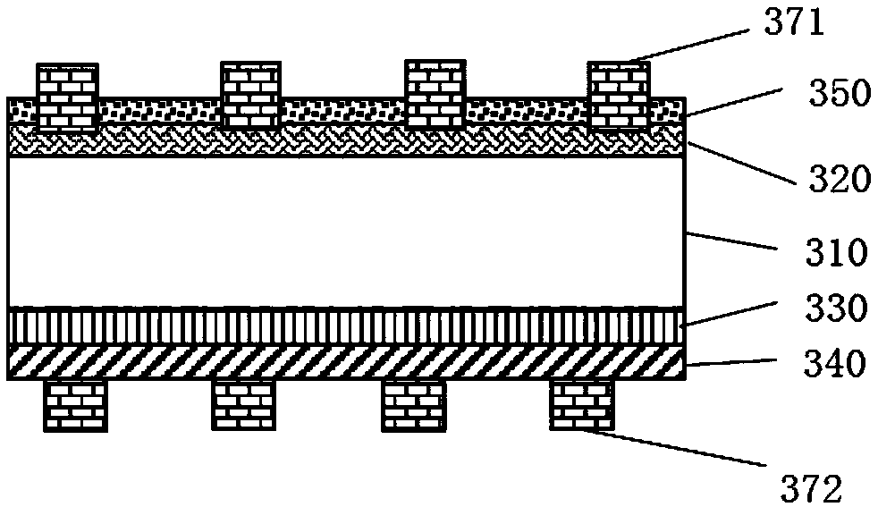
[0054] image 3 Another example diagram illustrating the fabrication of a solar cell according to an embodiment of the present invention.

[0055] In this embodiment, the crystalline silicon substrate 310 is an n-type crystalline silicon wafer, which may be a single crystal or polycrystalline silicon wafer. The n-type crystalline silicon substrate 310 is cleaned and textured. Phosphorus is diffused on the front side of the textured n-type crystalline silicon substrate 310 to form an n-type heavily doped crystalline silicon layer 320 .

[0056] Formation of SiN on the back of the cell using PECVD x The thickness of the tunneling thin film layer 330 is preferably 1-5 nm.

[0057] In SiO 2 The microcrystalline silicon layer 340 is deposited on the tunneling film layer 330 by PECVD or HWCVD, with a thickness of preferably 5-50 nm, and then the microcrystalline silicon layer 340 is doped with p-type by ion implantation.

[0058] Deposit 80-150nm SiN on the n-type heavily doped...


PUM

PropertyMeasurementUnit
Thicknessaaaaaaaaaa
Thicknessaaaaaaaaaa
Thicknessaaaaaaaaaa

Abstract

The invention discloses a passivation contact electrode structure and an applicable solar cell and a manufacturing method thereof. The electrode structure comprises a doped semiconductor layer and a copper electrode, wherein the doped semiconductor layer is deposited on a crystalline silicon substrate, the copper electrode is arranged on the doped semiconductor layer, the doped semiconductor is any one of polycrystalline silicon, microcrystalline silicon or microcrystalline silicon carbon alloy, and the thickness of the doped semiconductor is 5 to 100 nm. In an implementation process, the applicable solar cell is arranged on the back side or the two sides of the crystalline silicon substrate and comprises the passivation contact electrode structure. The invention further discloses a manufacturing of the solar cell with the passivation contact electrode structure. According to the passivation contact electrode structure disclosed by the invention, a surface composite efficiency of photo-induced carriers is reduced by passivating contact among all the metal electrodes, and a more complete passivation effect is achieved; meanwhile, compared with an existing technological method, massproduction of the passivation contact electrode structure disclosed by the invention is achieved; furthermore, electroplated copper is utilized as a conducting layer to replace silver, so that cell production cost is reduced.

Description

technical field [0001] The invention belongs to the field of solar batteries, and in particular relates to a passivation contact electrode structure, a suitable solar battery and a manufacturing method thereof. Background technique [0002] The working principle of solar cells is simply to extract photogenerated electron-hole pairs before their recombination and generate current. So how to reduce the recombination loss has always been one of the core points of solar cell research and development. Looking at the technical development route of silicon-based cells for more than two decades, reducing recombination loss and improving photogenerated electron / hole collection efficiency are the top priorities at any time, and proposed including aluminum back field passivation, using dielectric A series of technologies including front and back passivation of the film, high and low junction electric fields formed locally or on the entire surface, and heterojunction passivation. Howe...

Claims


Application Information

Patent Timeline
IPC IPC(8): H01L31/0224H01L31/20
CPCH01L31/022433H01L31/202H01L31/208Y02E10/50Y02P70/50
Inventor 李中天姚宇邓晓帆
Owner SUZHOU SUNWELL NEW ENERGY CO LTD
Why Eureka
Try Eureka