Organic light emitting diode, manufacturing method thereof, pixel structure and manufacturing method thereof

A technology of light-emitting diodes and organic light-emitting layers, which is applied in the field of pixel structure and its production, organic light-emitting diodes and its production, and can solve the problems that cannot be used to prepare organic light-emitting layers of RGB multi-color pixel arrays, uneven light emission of display pixels, and obstruction of space. Effective hole injection and other issues to achieve excellent luminous performance, high luminous uniformity, and low light-up voltage

Inactive Publication Date: 2018-11-13
SUZHOU INST OF NANO TECH & NANO BIONICS CHINESE ACEDEMY OF SCI
View PDF2 Cites 0 Cited by
  • Summary
  • Abstract
  • Description
  • Claims
  • Application Information

AI Technical Summary

Problems solved by technology

However, for organic light-emitting layer materials with deep highest occupied orbital (HOMO) energy levels (generally referring to HOMO energy levels between 5.5eV and 6.2eV), the relatively large energy level difference between PEDOT:PSS and them will greatly hinder the space Effective injection of holes
At the same time, when preparing the organic light-emitting layer of the

Method used


Image

  • Organic light emitting diode, manufacturing method thereof, pixel structure and manufacturing method thereof
  • Organic light emitting diode, manufacturing method thereof, pixel structure and manufacturing method thereof
  • Organic light emitting diode, manufacturing method thereof, pixel structure and manufacturing method thereof

Examples


Embodiment 1

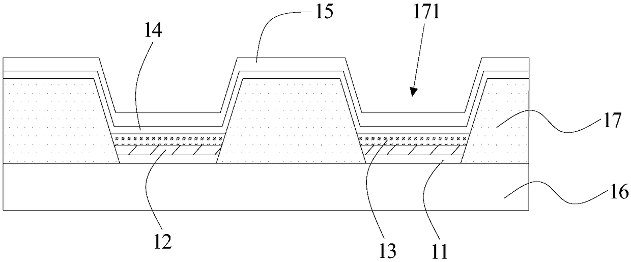
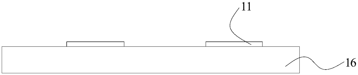
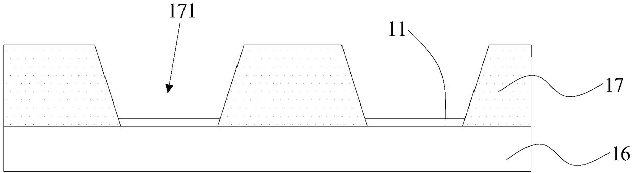
[0041] This embodiment provides an organic light emitting diode, specifically refer to figure 1 , according to the present embodiment, the organic light emitting diode comprises an anode 11, a hole injection layer 12, an organic light emitting layer 13, an electron transport layer 14 and a cathode 15 which are sequentially stacked; wherein, the work function of the material of the hole injection layer 12 is the same as The highest occupied orbital energy levels of the materials of the organic light emitting layer 13 are matched.

[0042] Specifically, the material of the organic light-emitting layer 13 is a polymer light-emitting material with the highest occupied orbital energy level of 5.5eV-6.2eV or an organic small molecule light-emitting material with a molecular weight of no more than 1000. Correspondingly, the material of the hole injection layer 12 The work function is controlled to be 5.5eV-6.0eV, which satisfies the matching between the two, so that excellent luminou...

Embodiment 2

[0064] In the description of Embodiment 2, the similarities with Embodiment 1 will not be repeated here, and only the differences with Embodiment 1 will be described. The difference between Example 2 and Example 1 is that in the organic light-emitting diode of Example 2, the material of the organic light-emitting layer is preferably poly[2-(4-(3 ', 7'-dimethyloctyloxy)-phenyl)-p-phenylene vinylene] (referred to as P-PPV), and the material of the hole injection layer is PEDOT:PSS:PFI with a work function of about 5.95eV, And in the PEDOT:PSS:PFI, the mass ratio of the three monomers PEDOT, PSS, and PFI is 1:6:1.6. Apparently, the material of the organic light-emitting layer in this embodiment can emit green light.

[0065] In the manufacturing method of the organic light emitting diode in this embodiment, the difference from the manufacturing method of the organic light emitting diode in embodiment 1 is that in step S2, the three monomers PEDOT and PSS are printed on the anode...

Embodiment 3

[0068] In the description of Embodiment 3, the similarities with Embodiment 1 will not be repeated here, and only the differences with Embodiment 1 will be described. The difference between embodiment 3 and embodiment 1 is that in the manufacturing process of the organic light emitting diode of this embodiment, in step S1, a flexible transparent conductive polyimide (referred to as PI) is used as the anode electrode substrate, one of which is On the one hand, it acts as a substrate, and on the other hand, it acts as a conductive anode; for the rest, refer to the manufacturing method described in Example 1 to obtain an organic light-emitting diode.

[0069] The maximum luminance of the organic light emitting diode obtained in this embodiment is 5000cd / m 2 ~5500cd / m 2 , the maximum current efficiency is 7cd / A, and the lighting voltage is 5V; the organic light emitting diode provided in this embodiment shows excellent luminous performance.


PUM

PropertyMeasurementUnit
Work functionaaaaaaaaaa
Thicknessaaaaaaaaaa

Abstract

The invention discloses an organic light emitting diode. The organic light emitting diode comprises an anode, a hole injection layer, an organic light emitting layer, an electron transport layer and acathode which are sequentially stacked; the work function of the hole injection layer is matched with the highest occupied molecular orbital energy level of the organic light emitting layer. The invention also discloses a pixel structure. The pixel structure comprises a red sub-pixel, a green sub-pixel and a blue sub-pixel arranged in sequence; each of the red sub-pixel, the green sub-pixel and the blue sub-pixel includes an anode, a hole injection layer, an organic light emitting layer, an electron transport layer and a cathode which are sequentially stacked; and in each of the red sub-pixel, the green sub-pixel and the blue sub-pixel, the work function of the hole injection layer is matched with the highest occupied molecular orbital energy level of the organic light emitting layer. According to the organic light emitting diode and the pixel structure of the invention, materials and printing processes are rationally selected during the manufacturing process of the organic light emitting diode and the pixel structure, and therefore, the work functions of the hole injection layers can be matched with the highest occupied molecular orbital energy level of the materials of the organic light emitting layers respectively, so that the organic light emitting diode and the pixel structure can realize excellent light emitting properties.

Description

technical field [0001] The invention belongs to the technical field of light-emitting diodes, and specifically relates to an organic light-emitting diode and a manufacturing method thereof, as well as a pixel structure and a manufacturing method thereof. Background technique [0002] Organic light-emitting diodes (OLEDs) are considered to be the third-generation display technology to replace liquid crystal displays (LCDs) due to their many advantages such as self-luminescence, high contrast, low power consumption, wide viewing angle, short response time, and the ability to prepare flexible devices. OLED is a stacked electroluminescent device with a "sandwich" structure, and its structure generally includes an anode, a hole injection (transport) layer, an organic light-emitting layer, an electron transport layer and a cathode. Wherein, the energy level difference between the hole injection layer and the organic light-emitting layer determines the difficulty of hole injection....

Claims


Application Information

Patent Timeline
IPC IPC(8): H01L51/50H01L51/54H01L51/56H01L27/32
CPCH10K59/35H10K71/13H10K85/1135H10K50/11H10K2101/40H10K50/17H10K71/00
Inventor 张东煜陈文斌苏文明郭文瑞
Owner SUZHOU INST OF NANO TECH & NANO BIONICS CHINESE ACEDEMY OF SCI
Why Eureka
Try Eureka