TFT substrate and manufacturing method thereof

A manufacturing method and substrate technology, which can be applied to electrical components, electrical solid devices, circuits, etc., can solve the problems of metal electrode line leftover, film breakage of passivation layer structure, short circuit, etc., and achieve excellent blocking effect.

Active Publication Date: 2018-11-23
SHENZHEN CHINA STAR OPTOELECTRONICS TECH CO LTD
View PDF7 Cites 1 Cited by
  • Summary
  • Abstract
  • Description
  • Claims
  • Application Information

AI Technical Summary

Problems solved by technology

However, when the source / drain metal layer of Cu / Mo is etched to form the source / drain by wet process, a galvanic cell is formed between Cu, Mo and the etching solution to cause corrosion of Cu
like figure 2 As shown in the enlarged frame of the middle dotted line, Cu is hollowed out, and the hollowed out part may cause etching solution to remain and further affect the channel of the active layer. When the upper layer of the chemical layer needs to be deposited and etched to form structures such as metal electrode lines, it may cause these metal electrode lines to remain at the broken film and cause a short circuit or a short circuit with the source / drain

Method used


Image

  • TFT substrate and manufacturing method thereof
  • TFT substrate and manufacturing method thereof
  • TFT substrate and manufacturing method thereof

Examples


Embodiment Construction

[0036] In order to further illustrate the technical means adopted by the present invention and its effects, the following describes in detail in conjunction with preferred embodiments of the present invention and accompanying drawings.

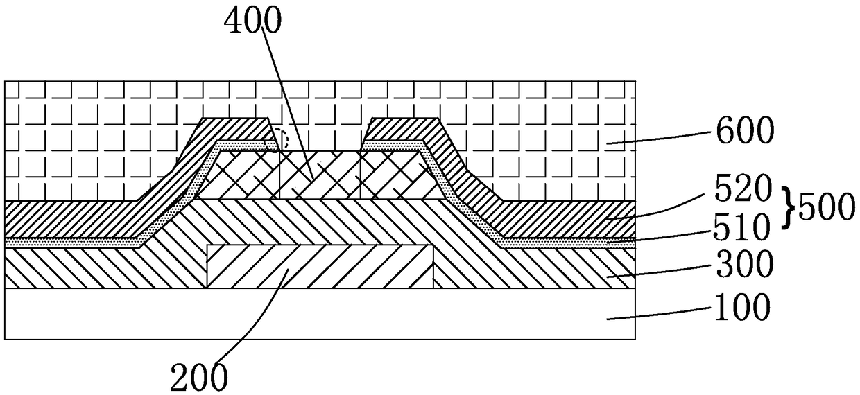
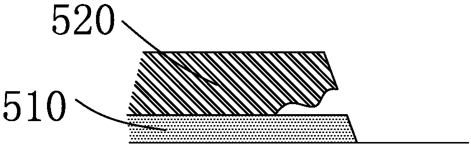
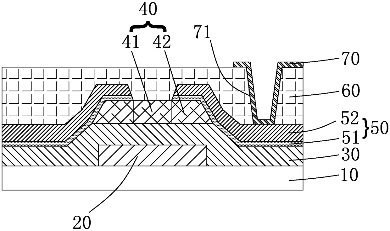
[0037] see image 3 , the present invention provides a TFT substrate, comprising a base substrate 10, a gate 20 disposed on the base substrate 10, a gate insulating layer 30 disposed on the base substrate 10 and the gate 20, a gate insulating layer 30 disposed on the gate insulating The layer 30 corresponds to the active layer 40 above the gate 20 , the source / drain 50 disposed on both sides of the active layer 40 , and the passivation layer 60 covering the source / drain 50 .

[0038] Wherein, the base substrate 10 is a transparent substrate, such as glass or quartz.

[0039] The gate 20 is a single-layer metal film or a multi-layer metal film, and its material is copper (Cu), aluminum (A1), molybdenum (Mo), titanium (Ti), silver (Ag), gold (A...


PUM


Abstract

The invention provides a TFT substrate and a manufacturing method thereof. The source / drain of the TFT substrate disclosed by the invention comprises a metal layer and a barrier layer formed by an inorganic amorphous conductive material or an organic conductive material; wherein the barrier layer is arranged between a source / drain contact region of an active layer and the metal layer of the source / drain. Due to the isotropy of the inorganic amorphous conductive material or the organic conductive material, a diffusion channel similar to a grain boundary is not formed, therefore, the diffusion of the source / drain metal atoms to the active layer can be blocked; meanwhile, a potential difference is not generated during the wet etching process of forming the source / drain, therefore, the metal layer can be prevented from being electrochemically corroded.

Description

technical field [0001] The invention relates to the field of display technology, in particular to a TFT substrate and a manufacturing method thereof. Background technique [0002] The flat panel display device has many advantages such as thin body, power saving, and no radiation, and has been widely used. Existing flat panel display devices mainly include Liquid Crystal Display (LCD) and Organic Light Emitting Display (OLED). [0003] Both liquid crystal displays and organic electroluminescence displays require TFT (Thin Film Transistor, thin film transistor) substrates and are driven by TFF elements on the TFT substrates. Therefore, thin film transistors, as the main driving elements in current liquid crystal display devices and active matrix OLED display devices, are directly related to the development direction of high-performance flat panel display devices. [0004] Taking the bottom-gate thin film transistor as an example, figure 1 It is a schematic structural diagra...

Claims


Application Information

Patent Timeline
Patent Type & Authority Applications(China)
IPC IPC(8): H01L27/12
CPCH01L27/1214H01L27/1237H01L27/127
Inventor 尹易彪
Owner SHENZHEN CHINA STAR OPTOELECTRONICS TECH CO LTD
Why Eureka
Try Eureka