Optical phased array chip transmitter based on metal slit waveguides

An optical phased array and slotted waveguide technology, applied in the field of integrated optics, can solve the problems of small beam scanning angle, large waveguide spacing, weak light wave mode field constraints, etc., achieve large beam deflection angle, small crosstalk, and increase deflection angle range Effect

Inactive Publication Date: 2018-11-27
SHANGHAI JIAO TONG UNIV +1
View PDF8 Cites 5 Cited by
  • Summary
  • Abstract
  • Description
  • Claims
  • Application Information

AI Technical Summary

Problems solved by technology

[0006] It can be seen that the phased array technology based on the dielectric optical waveguide is now used to realize the beam steering. Due to the weak constraint of the waveguide on the optical wave mode field, the distance between the waveguides is relatively large and cannot be smaller than the half-wave wavelength, so the beam scanning angle is small.

Method used


Image

  • Optical phased array chip transmitter based on metal slit waveguides
  • Optical phased array chip transmitter based on metal slit waveguides
  • Optical phased array chip transmitter based on metal slit waveguides

Examples


Embodiment

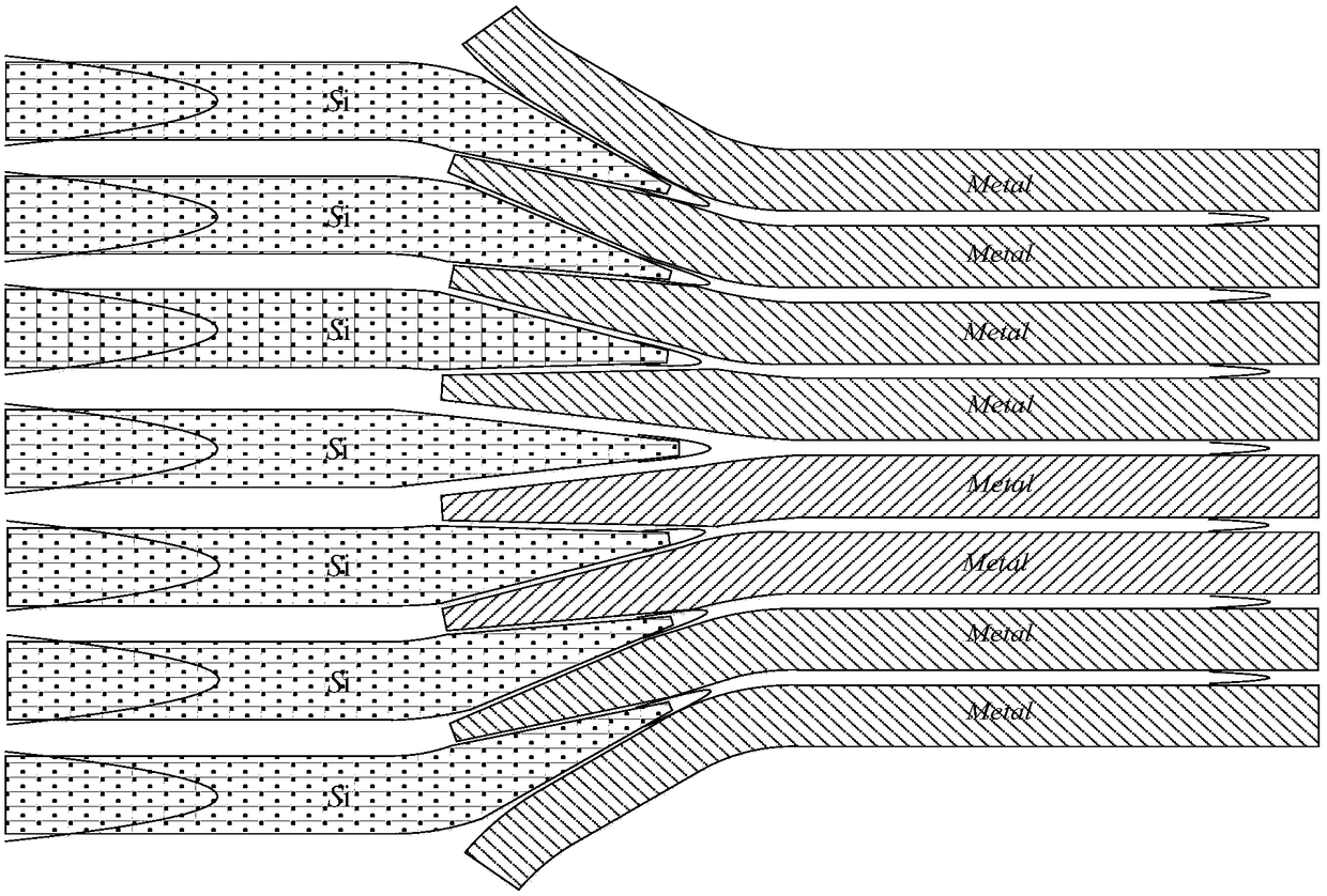
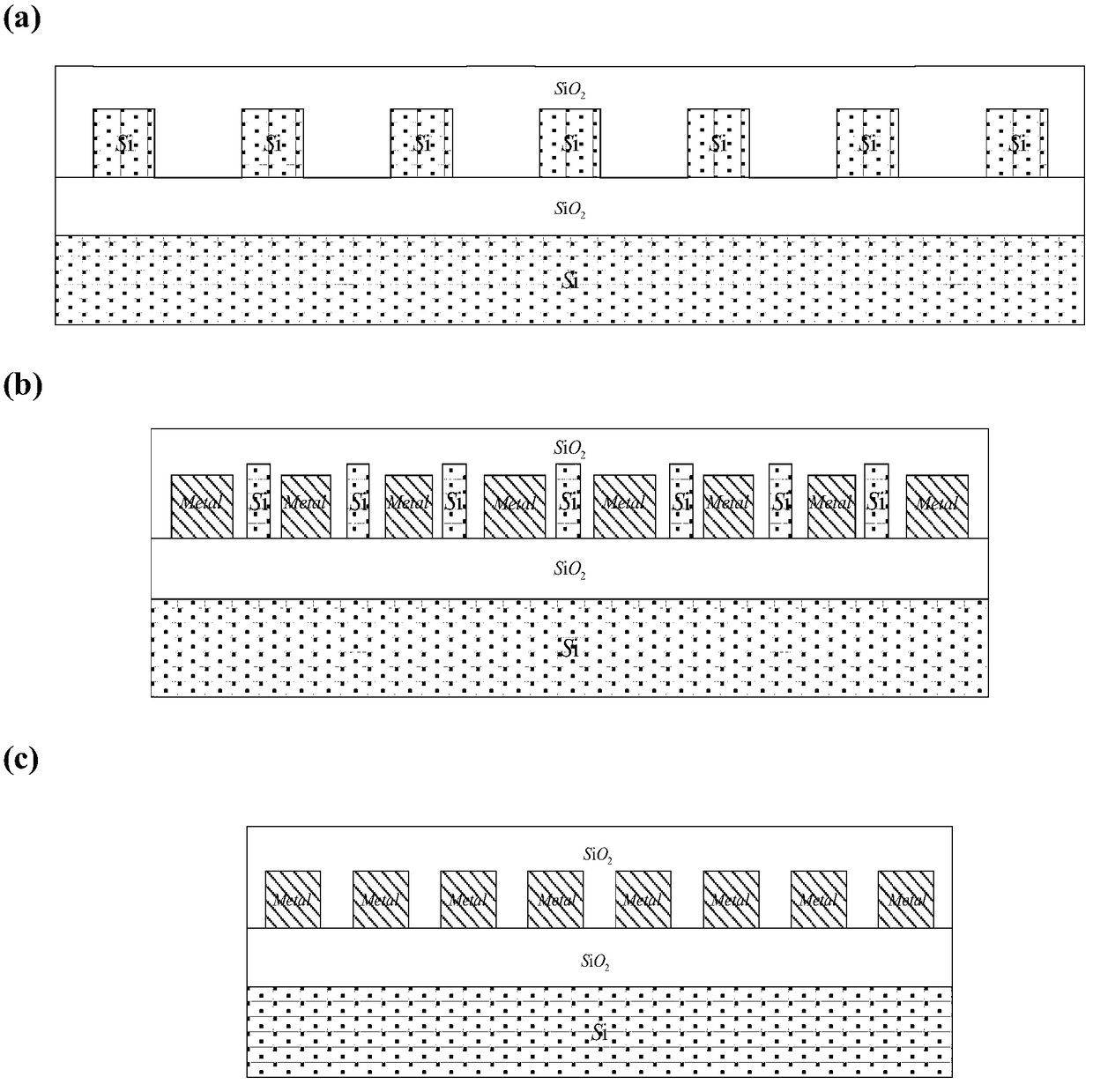
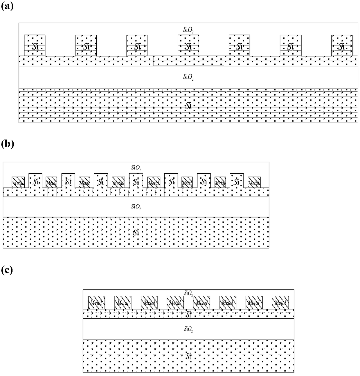
[0023] figure 2 and image 3The thickness of the middle and lower cladding layers is 2μm, the thickness of the upper cladding layer is 1.5μm, the thickness of the silicon waveguide layer is 220nm, the width of the left waveguide layer is 500nm, and the center interval of the waveguide is 5μm. Among them, image 3 The thickness of the slab layer of the middle silicon waveguide is 90nm, and the thickness of the convex part is 130nm. figure 1 The distance between the edges of adjacent metal plasmonic slot waveguides at the position of the dotted line on the right side of the center is 100nm, figure 2 The thickness of the metal plasmonic slot waveguide is 170nm, image 3 The thickness of the metal plasmonic slot waveguide is 90nm. The distance between the edges of adjacent waveguides in the interspersed part of the silicon waveguide and the metal plasma slot waveguide is 50nm, the minimum width of the tapered part at the far right end of the silicon waveguide is 80nm, and the...


PUM


Abstract

The invention discloses an optical phased array chip transmitter based on metal slit waveguides. The transmitter is formed by a medium optical waveguide array and a metal plasma slit waveguide array.The interval of the medium optical waveguides is gradually reduced from the left to the right, and the whole medium optical waveguide is of a fan-shaped structure. The interval of the metal plasma slit waveguide array is firstly reduced and then unchanged, and the whole metal plasma slit waveguide array likes a transversely arranged hopper. The right end of the medium optical waveguide array and the left end of the metal plasma slit waveguide array form a whole body structure in a penetrating way, so it is ensured that optical energy is transited to the metal plasma waveguide from the medium waveguide in a low loss manner. According to the invention, by use of the characteristics of weak penetrating ability of light in metal and strong light wave model field constraints, intervals of the plasma waveguides are reduced, the range of output diffraction angle is increased, and the laser scanning angle covering range is increased. The emission end is simple in structure, small in crosstalkbetween waveguides, and big output wave beam deflection angle and has profound application prospects in laser radar field.

Description

technical field [0001] The invention relates to optical phased array technology and on-chip laser radar technology, and belongs to the field of integrated optics. Background technique [0002] Lidar is a new type of active radar integrating modern optical remote sensing, imaging, ranging, tracking and other technologies. It is the product of the combination of traditional radar technology and modern laser technology. Because of the characteristics of high correlation, good monochromaticity and high brightness of laser, the application of laser to radar has the advantages of high resolution, wide measurement range and strong anti-interference performance, so it has attracted extensive attention from researchers. With the maturity of technology and the improvement of manufacturing process, lidar will become an indispensable part of the development of future communication, ranging and other technologies. In addition to military applications, lidar can also be used for navigati...

Claims


Application Information

Patent Timeline
Patent Type & Authority Applications(China)
IPC IPC(8): G01S7/481
CPCG01S7/4814
Inventor 陆梁军孙乾坤周林杰陈建平厐拂飞
Owner SHANGHAI JIAO TONG UNIV
Why Eureka
Try Eureka