LED chip and cutting method thereof

A technology of LED chips and cutting methods, which is applied to electrical components, circuits, abrasives, etc., can solve problems such as low yield rate, abnormal photoelectric characteristics, and low luminous efficiency of LED chips, so as to improve yield rate, avoid edge cracking, and overall luminescence The effect of improving efficiency

Active Publication Date: 2018-11-27
YANGZHOU CHANGELIGHT
View PDF4 Cites 5 Cited by
  • Summary
  • Abstract
  • Description
  • Claims
  • Application Information

AI Technical Summary

Problems solved by technology

[0004] In view of this, the present invention provides an LED chip and its cutting method to solve the problems of low luminous efficiency, abnormal photoelectric characteristics and low yield of LED chips obtained by the chip cutting method (scribing method) in the prior art.

Method used


Image

  • LED chip and cutting method thereof
  • LED chip and cutting method thereof
  • LED chip and cutting method thereof

Examples


Embodiment Construction

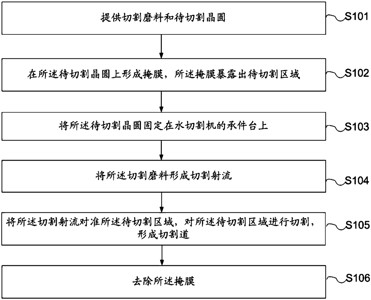
[0041] As mentioned in the background technology section, the LED chips obtained by the chip dicing method in the prior art have low luminous efficiency, abnormal photoelectric characteristics, and a low yield rate.

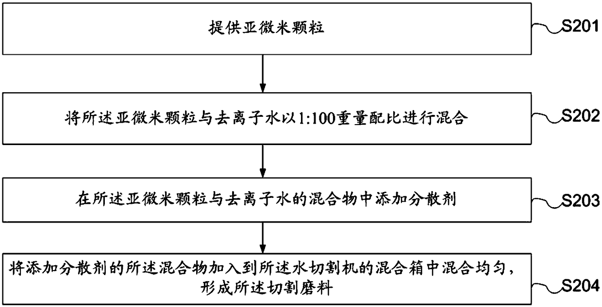
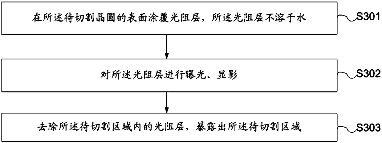
[0042] The inventors found that the reason for the above phenomenon is that the epitaxial layer of the LED wafer is mostly brittle materials such as AlGaInP, GaAs, GaP; The phenomenon of edge chipping and the generation of cutting residue; resulting in a decrease in yield. Moreover, the severity of cracking is closely related to the use status of the blade, which will cause inconsistency in the cutting quality of the product; and during the high-energy thermal processing of the laser, the high-temperature molten residue splashed out conducts the PN junction in the LED chip, causing the LED chip to leak electricity , In addition, because the black molten residue adhering to the side wall of the chip will block the emission of light, the overall luminous efficiency...


PUM

PropertyMeasurementUnit
particle diameteraaaaaaaaaa
diameteraaaaaaaaaa
thicknessaaaaaaaaaa

Abstract

The invention discloses an LED chip and a cutting method thereof. The cutting method of the LED chip provided by the invention is characterized in that after a cutting grinding material is prepared, the cutting grinding material is pressurized to form high-pressure cutting jet through a pressurization system in a waterjet cutting machine, so that the high-pressure cutting jet acts on the surface of an LED wafer, so that the goal of cutting the LED wafer is achieved. The LED chip cutting method provided by the invention is a cold cutting mode, so that the heat influence cannot be generated in the cutting process; melts similar to that in laser cutting cannot be generated, so that the condition that the LED chip leaks electricity or is shielded by the melts is effectively avoided; the LED lateral wall light outlet is favorably realized; the luminous efficiency of the LED chip is improved. In addition, the high pressure jet effect is fluid stress and is not mechanical stress, so that thephenomenon of edge crack in the chip cutting process is avoided; the qualification rate of the LED chip is improved.

Description

technical field [0001] The invention relates to the technical field of manufacturing semiconductor chips, in particular to an LED chip and a cutting method thereof. Background technique [0002] The manufacture of LED (Light Emitting Diode, light-emitting diode) chips starts from a complete wafer, after a series of processes such as chemical cleaning, evaporation, photolithography, etc., and finally undergoes scribing and splitting processes, and becomes separated one by one. Chip; the current LED chip slicing methods used in the industry are mainly divided into two types: one is to use a hub-shaped blade embedded with diamond abrasives on the edge to cut the surface material of the LED chip under high-speed rotation; the other is The high-energy beam generated by the laser is used to melt the surface material of the LED chip and then sputter it to form a cutting line. [0003] However, the LED chips obtained by the chip dicing method in the prior art have low luminous effi...

Claims


Application Information

Patent Timeline
Patent Type & Authority Applications(China)
IPC IPC(8): H01L21/78H01L33/00B24C1/04B24C3/00
CPCB24C1/045B24C3/00H01L21/78H01L33/00
Inventor 石峰杜俊康徐洲赵鹏王涛
Owner YANGZHOU CHANGELIGHT
Why Eureka
Try Eureka