MWT solar cell and preparation method thereof
A technology for solar cells and electrodes, applied in the field of solar cells, can solve the problems of difficult passivation of the n+ surface and doping of the whole surface of the polysilicon film, and achieve the effect of solving the problems of short circuit and leakage
- Summary
- Abstract
- Description
- Claims
- Application Information
AI Technical Summary
Problems solved by technology
Method used
Image

Examples
Embodiment 1
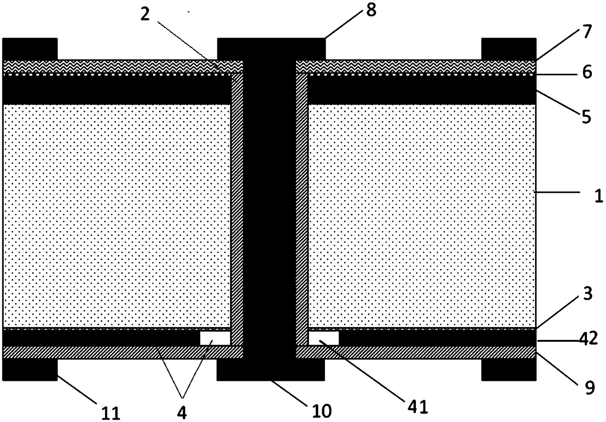
[0086] Such as figure 1 As shown, the MWT solar cell provided in this implementation includes an n-type silicon substrate 1, in which a through hole 2 leading the front electrode to the back is provided, and a dielectric film 3 is provided on the back of the n-type silicon substrate 1 , the dielectric film 3 is provided with a selectively doped polysilicon film 4, the selectively doped polysilicon film 4 includes a non-doped polysilicon film 41 and a doped polysilicon film 42, the non-doped polysilicon film 41 surrounds the through hole 2, and the remaining area Then it is the doped polysilicon film 42 .
[0087] from figure 1 It can be known from the structure of the solar cell that the through hole 2 is surrounded by the non-doped polysilicon film 41, which can electrically insulate and isolate the lead in the through hole 2 for connecting the front electrode to the back, thereby reducing or avoiding leakage and short circuit.
[0088] The region of the non-doped polysilic...
Embodiment 2
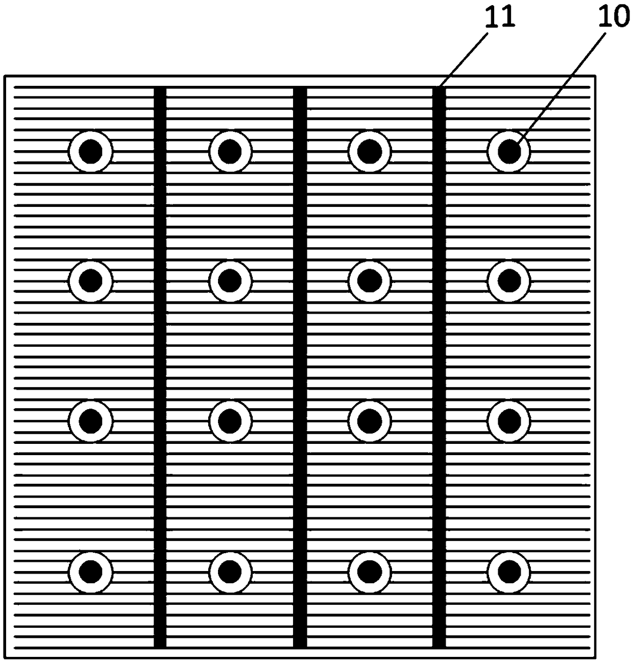
[0116] The difference from Example 1 is that in this MWT solar cell, the back contact electrode 11 is a whole-surface metal electrode except the front electrode.
[0117] The dielectric film 3 is a silicon dioxide monolayer film with a thickness of 1.5 nm.
[0118] The doped polysilicon film is a phosphorus-doped polysilicon film, and its doping concentration is 1.0E 19 atoms / cm 3 -2.0E 21 atoms / cm 3 , with a thickness of 80nm.
[0119] The preparation method of this MWT solar cell, this method is to realize boron doping based on boron diffusion, low pressure chemical deposition (LPCVD) prepares a layer of silicon dioxide (SiO 2 ) ultra-thin dielectric film, local ion implantation is performed on the polysilicon film on it to realize local area selective phosphorus (P) doping, and the entire metal electrode is printed on the n+ doped polysilicon, and its pattern is as follows Image 6 , forming a unique single-sided n-type MWT battery, which can not only make secondary us...
Embodiment 3
[0133] The difference from Example 1 is that in this MWT solar cell, the back contact electrode 11 is a whole-surface metal electrode except the front electrode.
[0134] Dielectric film 3 is silicon oxynitride (SiO x N 1-x ) ultra-thin dielectric film with a thickness of 0.5nm.
[0135] The doped polysilicon film is a phosphorus-doped polysilicon film, and its doping concentration is 1.0E 19 atoms / cm 3 -2.0E 21 atoms / cm 3 , with a thickness of 60nm.
[0136] The preparation method of this MWT solar cell, this method is to prepare a layer of silicon oxynitride (SiO2) based on low pressure chemical deposition (LPCVD). x N 1-x ) ultra-thin dielectric film, local ion implantation is performed on the polysilicon layer above it, and boron ion implantation is performed on the front side, and local area selective phosphorus (P) doping and boron (B) doping are realized through a one-step annealing process. In n+ Doped polysilicon prints the entire metal electrode to form a uni...
PUM
 Abstract
Description
Claims
Application Information
 - R&D
- Intellectual Property
- Life Sciences
- Materials
- Tech Scout
- Unparalleled Data Quality
- Higher Quality Content
- 60% Fewer Hallucinations
Browse by: Latest US Patents, China's latest patents, Technical Efficacy Thesaurus, Application Domain, Technology Topic, Popular Technical Reports.
© 2025 PatSnap. All rights reserved.Legal|Privacy policy|Modern Slavery Act Transparency Statement|Sitemap|About US| Contact US: help@patsnap.com