Laser processing equipment, three-dimensional antenna, processing method and communication equipment

A three-dimensional antenna, laser processing technology, applied in laser welding equipment, metal processing equipment, welding equipment and other directions, can solve the problems of low component flexibility, short preparation process, long preparation process, etc., to improve processing efficiency and improve processing accuracy , the effect of extending the connection method

Inactive Publication Date: 2018-12-07
SHANGHAI AMPHENOL AIRWAVE COMM ELECTRONICS CO LTD
View PDF8 Cites 1 Cited by
  • Summary
  • Abstract
  • Description
  • Claims
  • Application Information

AI Technical Summary

Problems solved by technology

Therefore, the layout of the components on the circuit board of the existing antenna assembly or the design of the existing antenna assembly will be limited by the PCB or FPC, which limits the application range of the antenna assembly. When designing the antenna, it is necessary to first consider the PCB or FPC, component placement less flexible
[0003] In addition, the PCB preparation process is long and the cost is high. In some specific antenna line applications, people need to find a new process route with a short preparation process and low cost.

Method used


Image

  • Laser processing equipment, three-dimensional antenna, processing method and communication equipment
  • Laser processing equipment, three-dimensional antenna, processing method and communication equipment
  • Laser processing equipment, three-dimensional antenna, processing method and communication equipment

Examples


Embodiment 1

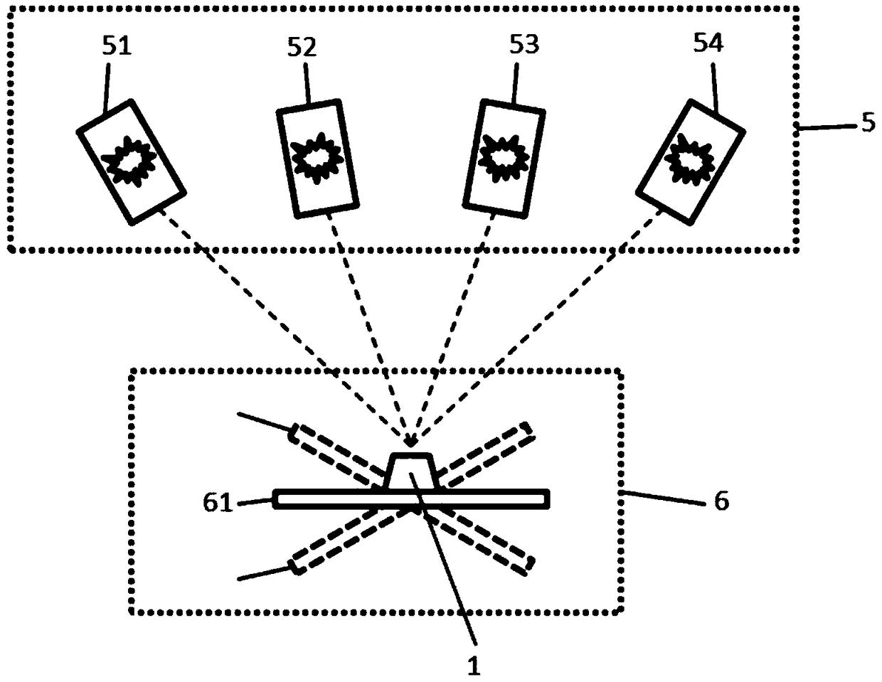
[0053] see figure 1 , a laser processing equipment for a three-dimensional antenna, comprising: a laser light source 5 for laser processing an insulating substrate 1 of a three-dimensional antenna to obtain a routing path of a metal circuit of the three-dimensional antenna; and a positioning unit 6 for Insulating base material 1 is positioned and fixed insulating base material 1; And the stereoscopic optical vision detection unit (not shown) that is used for positioning and detecting insulating base material 1; And the linearity that is used to adjust the position of insulating base material 1 motor (not shown in the figure); wherein, the number of laser light sources 5 is multiple; the positioning unit 6 has multiple switchable processing stations 61 , and the multiple processing stations 61 correspond to multiple laser light sources 5 .

[0054] The laser processing equipment of the three-dimensional antenna in the present embodiment includes a plurality of laser light sourc...

Embodiment 2

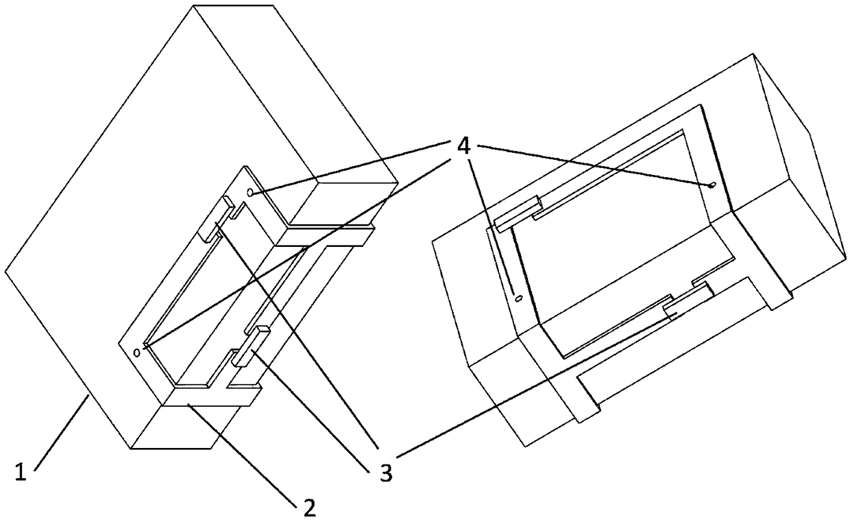
[0060] see figure 2 , a three-dimensional antenna, comprising: an insulating substrate 1, used to provide the stability of the overall structure of the three-dimensional antenna; several surface mount components 3, the surface mount components 3 are arranged on the outer surface of the insulating substrate 1; and metal circuits 2. The metal line 2 is arranged on the outer surface of the insulating substrate 1, and the metal line 2 is electrically connected to the surface mount component 3; wherein, the number of metallized via holes is one or more, and the diameter of the metallized via holes is less than 0.5 mm; the metal circuit 2 is directly formed on the insulating substrate 1 . The material of the metal circuit 1 can be any combination of copper and nickel, copper and silver, copper and nickel and gold, copper and nickel and tin.

[0061] In the three-dimensional antenna in this embodiment, the metal circuit 2 is directly formed on the insulating substrate 1, and the su...

Embodiment 3

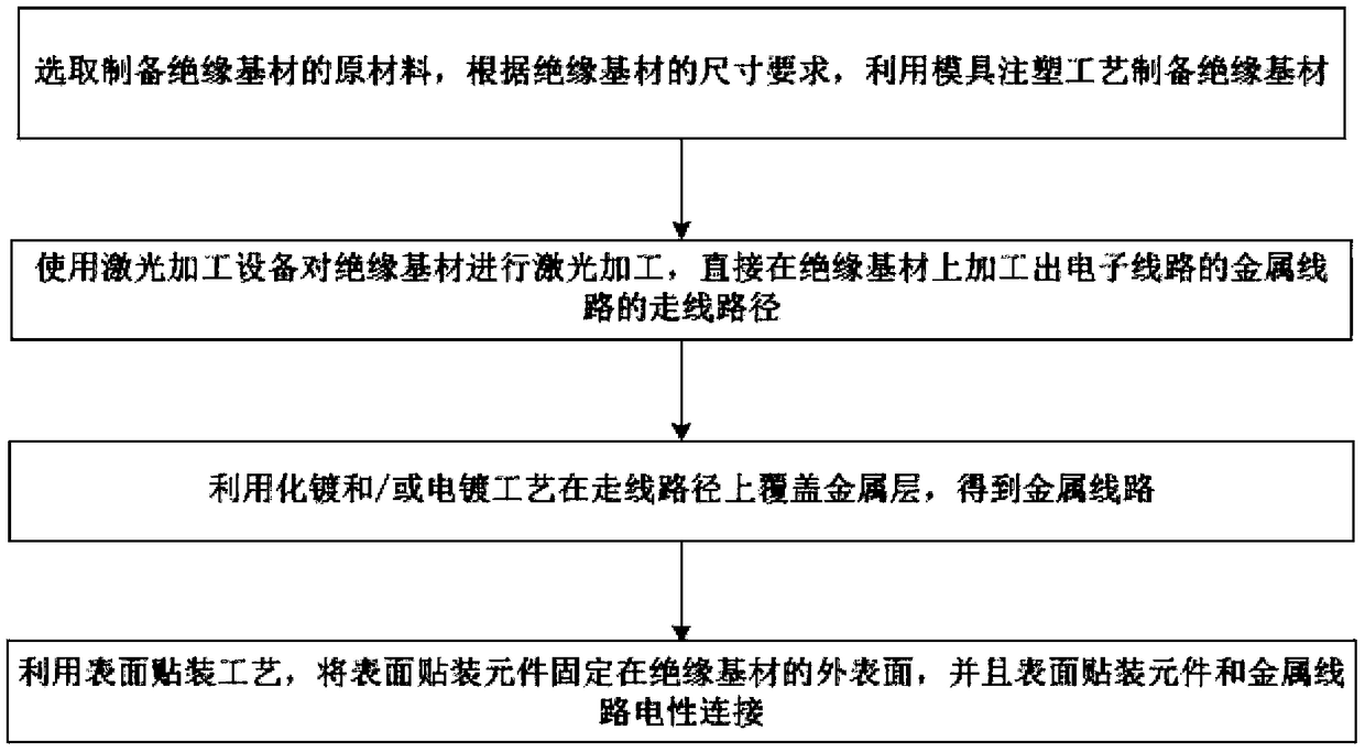
[0066] see image 3 , a processing method for a three-dimensional antenna, comprising: S1: selecting raw materials for preparing an insulating base material, and preparing the insulating base material by using a mold injection molding process according to the size requirements of the insulating base material; S2: using the laser of the three-dimensional antenna in Example 1 The processing equipment performs laser processing on the insulating substrate, and directly processes the routing path of the metal circuit of the three-dimensional antenna on the insulating substrate; S3: uses electroless plating and / or electroplating technology to cover the metal layer on the routing path to obtain a metal circuit ; S4: Using a surface mount process, the surface mount component is fixed on the outer surface of the insulating substrate, and the surface mount component is electrically connected to the metal circuit.

[0067] Specifically, step S2 includes a surface engraving process, an ed...


PUM

PropertyMeasurementUnit
wavelengthaaaaaaaaaa

Abstract

The invention discloses laser processing equipment of a three-dimensional antenna. The laser processing equipment comprises laser sources, a locating unit, a three-dimensional optical vision detectionunit and a linear motor. The laser source is used for carrying out laser processing on an insulation substrate of the three-dimensional antenna so as to obtain the running path of metal lines of thethree-dimensional antenna. The locating unit is used for locating and fixing the insulation substrate. The multiple laser sources are arranged, the locating unit is provided with multiple processing stations capable of being switched, and the multiple processing stations correspond to the multiple laser sources. The invention further discloses the three-dimensional antenna, a processing method andcommunication equipment.

Description

technical field [0001] The invention belongs to the field of antenna design, and in particular relates to a laser processing device for a three-dimensional antenna, a three-dimensional antenna, a processing method and a communication device. Background technique [0002] With the wide application of antennas and the development of new technologies, new requirements are put forward for the design of antennas and the equipment for processing antennas. In some existing antenna assemblies, surface mount components are attached to upper and lower surfaces of a printed circuit board (PCB for short) or a flexible printed circuit board (FPC for short) to form an antenna assembly. Because both PCB and FPC are chip or multi-layer chip structures, surface mount components can only be attached to the outermost surface of one side or the upper and lower sides of the PCB. Therefore, the layout of the components on the circuit board of the existing antenna assembly or the design of the ex...

Claims


Application Information

Patent Timeline
Patent Type & Authority Applications(China)
IPC IPC(8): B23K26/00H01Q1/38
CPCB23K26/00H01Q1/38
Inventor 蒋海英吴昊姜来新
Owner SHANGHAI AMPHENOL AIRWAVE COMM ELECTRONICS CO LTD
Why Eureka
Try Eureka