Ga2O3-based transparent conducting thin film and preparation method thereof
A transparent conductive film, ta2o5 technology, applied in ion implantation plating, metal material coating process, coating and other directions, can solve problems such as limited improvement
- Summary
- Abstract
- Description
- Claims
- Application Information
AI Technical Summary
Problems solved by technology
Method used
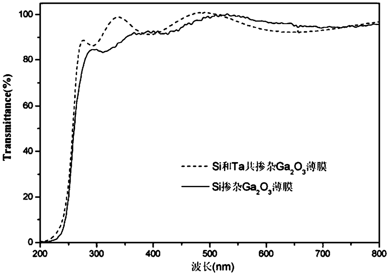
Image

Examples
Embodiment 1
[0047] 1) Using high temperature atmosphere sintering method to obtain high density Si and Ta doped Ga 2 o 3 Mixed target, the specific process includes: a) choose nano-Ga with a purity higher than 99.99% and a particle size of 40nm 2 o 3 powder, nano-SiO 2 Powder and Nano Ta 2 o 5 powder, mix and grind for 1 hour according to the weight ratio of 98.9:1:0.1, then add 1 wt% PVA for grinding and granulation, then put the granulated powder into the hydraulic press mold and keep the pressure under 40MPa pressure for 5 minutes to obtain the initial Blank. b) After the green body is degreased in a 600°C incubator, it is subjected to 350MPa cold isostatic pressing secondary molding treatment, and the pressure is maintained for 1.5 minutes to obtain a green body. c) Carry out high-temperature sintering to the biscuit in an oxygen environment (pressure 0.02MPa), the sintering temperature is 1400°C, and the holding time is 9 hours. Finally, Si and Ta doped Ga with a density of 88...
Embodiment 2
[0051] The substrate used in this example is a (0001) plane sapphire substrate instead of the homogeneous Ga 2 o 3 substrate, so this embodiment is heterogeneous substrate deposition Ga 2 o 3 film. The specific implementation process is as follows:
[0052] 1) Obtain Si and Ta doped Ga with high density (better than 85%) according to the method of Example 1 2 o 3 mixed target.
[0053] 2) First, a layer of Ga is deposited on the (0001) plane sapphire substrate at low temperature by laser pulse deposition process. 2 o 3 Nucleation layer material, and then deposit a layer of Ga at high temperature 2 o 3 base transparent conductive film. Specific steps are as follows:
[0054] A) Clean the surface of the sapphire substrate first, remove the surface grease, rinse with deionized water and blow dry with nitrogen, and put it into the heated substrate holder of the laser pulse deposition chamber;
[0055] B) A commercially available nucleation layer material target (pure G...
PUM
| Property | Measurement | Unit |
|---|---|---|
| Thickness | aaaaa | aaaaa |
| Carrier concentration | aaaaa | aaaaa |
Abstract
Description
Claims
Application Information