An organic light-emitting device and display panel
A technology of organic light-emitting devices and light-emitting layers, applied in organic semiconductor devices, electric solid-state devices, semiconductor devices, etc., can solve the problems of high price, low luminous efficiency, and blue phosphorescent materials that have not yet been commercialized, and achieve low prices , Improve luminous efficiency, improve the effect of luminous uniformity
- Summary
- Abstract
- Description
- Claims
- Application Information
AI Technical Summary
Problems solved by technology
Method used
Image
Examples
no. 1 example
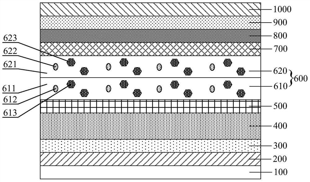
[0042] figure 1 It is a schematic structural diagram of an organic light emitting device according to the first embodiment of the present invention. From figure 1 It can be seen from the figure that the organic light emitting device of the embodiment of the present invention includes a first electrode 200 , a second electrode 1000 and a light emitting layer 600 . Wherein, the second electrode 1000 is disposed opposite to the first electrode 200 , and the light emitting layer 600 is disposed between the first electrode 200 and the second electrode 1000 . The material of the light-emitting layer 600 includes a host material, a luminescent guest and an auxiliary guest. The luminescent guest includes a fluorescent dye, and the auxiliary guest includes an organic compound with thermally activated delayed fluorescence (TADF) properties. The host material may include small molecule organic materials, such as CBP material (4,4'-bis(9-carbazole)biphenyl), mCBP material (3,3'-bis(9-ca...
no. 2 example
[0071] Figure 6 It is a schematic structural diagram of a top-emitting organic light-emitting device according to the second embodiment of the present invention. Different from the first embodiment, in this embodiment, if Figure 6 As shown, the light emitting surface is disposed on a side of the second electrode 1000 away from the first electrode 200 . The top emission organic light emitting device further includes a light extraction layer 1100, which is arranged on the side of the second electrode 1000 away from the light emitting layer 600, and the light extraction layer can increase the light extraction rate of the organic light emitting device and increase the brightness of the organic light emitting device. In a specific implementation, the material of the light extraction layer 1100 includes an organic material, an inorganic material or an organic-inorganic hybrid material with an average refractive index greater than or equal to 1.7 in the visible light range, su...
no. 3 example
[0077] Based on the inventive concepts of the foregoing embodiments, an embodiment of the present invention further provides a display panel, which includes the organic light emitting device of the foregoing embodiments, and further includes a thin film transistor for driving the organic light emitting device. The display panel can be any product or component with a display function such as a mobile phone, a tablet computer, a TV set, a monitor, a notebook computer, a digital photo frame, a navigator, and the like.
PUM
| Property | Measurement | Unit |
|---|---|---|
| thickness | aaaaa | aaaaa |
| refractive index | aaaaa | aaaaa |
Abstract
Description
Claims
Application Information


