

A process for using iodine lead formamidine as a light absorbing layer of a solar cell and an application thereof
A technology of solar cells and lead formamidine, which is applied in the field of solar cells, can solve the problems that iodine lead formamidine is not effective and reduces activation energy, and achieves the effects of low cost, improved stability/life, and improved stability and life
- Summary
- Abstract
- Description
- Claims
- Application Information
AI Technical Summary
Problems solved by technology
Method used
Image

Examples
Embodiment 1
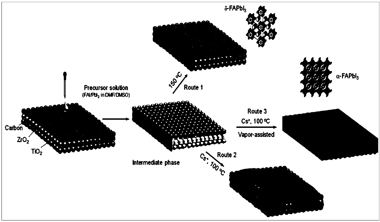
[0047] (1) On the FTO substrate, the transparent conductive layer, TiO 2 (such as NR18, NR30, P25) charge transport layer, insulating layer (ZrO 2 ) and a carbon electrode layer to prepare a blank device with a three-layer mesoporous membrane structure;
[0048] (2) Preparation of perovskite precursor: PbI2 and CsI, FAI were dissolved in a certain amount of DMF, and stirred evenly to obtain a clear and transparent precursor solution FAPbI with a perovskite content of 1M 3 ;
[0049] (3) Fill 3 μL of the precursor solution into the screen-printed blank device, let it stand still, and complete the preparation after annealing at 150° C. for 30 min in an atmosphere containing DMF and excluding DMSO.
Embodiment 2
[0051] (1) On the FTO substrate, the transparent conductive layer, TiO 2 (NR18, NR30, P25) charge transport layer, insulating layer (ZrO 2 ) and a carbon electrode layer to prepare a blank device with a three-layer mesoporous membrane structure;
[0052] (2) Preparation of perovskite precursor: PbI 2 and FAI were dissolved in a certain amount of DMF / DMSO (volume ratio of 6 / 1 to 4 / 1), and stirred evenly to obtain a clear and transparent precursor solution FAPbI with a perovskite content of 1M 3 ;
[0053] (3) Fill 3 μL of precursor solution into the screen-printed blank device, let it stand still, and complete the preparation after annealing at 150° C. for 30 min in a solvent atmosphere containing DMSO (that is, in a steam atmosphere containing DMSO).
Embodiment 3
[0055] (1) On the FTO substrate, the transparent conductive layer, TiO 2 (NR18, NR30, P25) charge transport layer, insulating layer (ZrO 2 ) and a carbon electrode layer to prepare a blank device with a three-layer mesoporous membrane structure;
[0056] (2) Preparation of perovskite precursor: PbI 2 and CsI, FAI were dissolved in a certain amount of DMF, and stirred evenly to obtain a clear and transparent precursor solution Cs with a perovskite content of 1M x FA 1-x PB 3 (x=0-0.15);
[0057] (3) Fill 3 μL of the precursor solution into the screen-printed blank device, let it stand still, and complete the preparation after annealing at 100° C. for 30 min.
PUM
 Abstract
Description
Claims
Application Information