Transverse groove-type MOSFET device and preparation method thereof

A technology of lateral trenches and devices, applied in semiconductor/solid-state device manufacturing, semiconductor devices, electrical components, etc., can solve the problems of low working speed, poor reliability, and high power loss

Active Publication Date: 2019-01-01
UNIV OF ELECTRONICS SCI & TECH OF CHINA
View PDF5 Cites 6 Cited by
  • Summary
  • Abstract
  • Description
  • Claims
  • Application Information

AI Technical Summary

Problems solved by technology

[0006] The present invention provides a lateral MOSFET device for the problems of poor long-term application reliability caused by excessively high gate dielectric layer elec

Method used


Image

  • Transverse groove-type MOSFET device and preparation method thereof
  • Transverse groove-type MOSFET device and preparation method thereof
  • Transverse groove-type MOSFET device and preparation method thereof

Examples


Embodiment 1

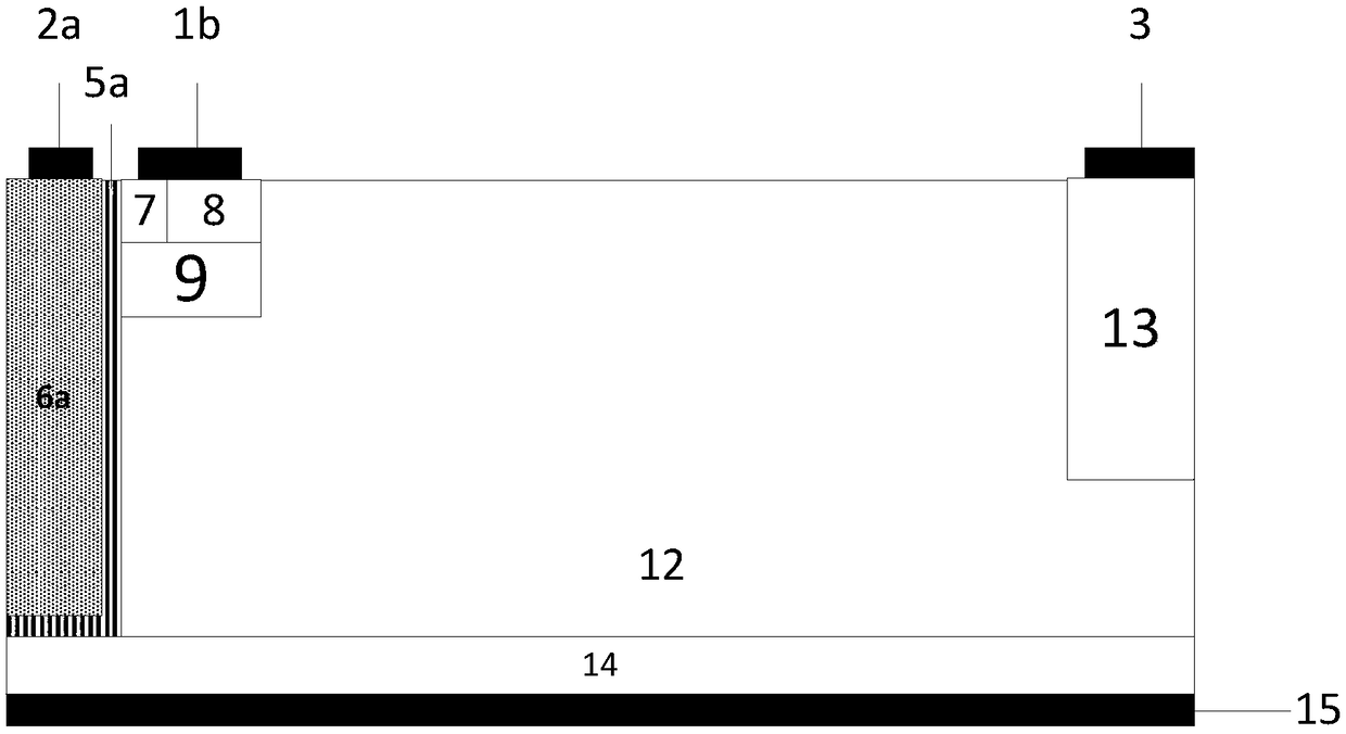
[0098] The lateral silicon carbide MOSFET provided by this embodiment has a device cell structure such as figure 2 As shown, it includes a silicon carbide P-type substrate 14 and a substrate electrode 15 arranged on the back of the silicon carbide P+ substrate 14; the front surface of the silicon carbide P+ substrate 14 is provided with silicon carbide whose upper and lower surfaces are flush and adjacent to the left and right. N-type doped region 11 and silicon carbide N-type drift region 12, the doping concentration of silicon carbide N-type doped region 11 is higher than that of silicon carbide N-type drift region 12; in the silicon carbide N-type drift region 12 The top layer is provided with a silicon carbide N+ drain region 13, and the upper surface of the silicon carbide N+ drain region 13 is provided with a drain metal 3; a polysilicon region is provided on the top layer of the silicon carbide N-type doped region 11 away from the drain metal 3 4. The upper and lower sur...

Embodiment 2

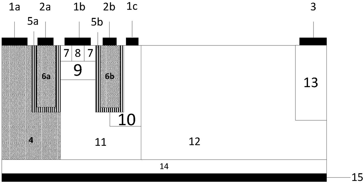
[0100] The lateral silicon carbide MOSFET provided by this embodiment has a device cell structure such as Figure 4 As shown, the difference from Embodiment 1 is that the substrate is an SOI substrate. The SOI substrate includes a BULK region 18, an SOI dielectric layer 17 and a silicon carbide N+ substrate 16 from bottom to top, such as Figure 4 Shown. This improvement not only isolates the substrate current, but also provides a low resistance channel for electrons, such as Figure 5 Shown. Therefore, the improvement is beneficial to improve the on-state performance of the device;

Embodiment 3

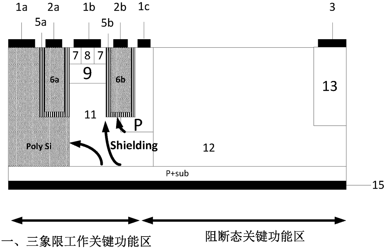
[0102] The lateral silicon carbide MOSFET provided by this embodiment has a device cell structure such as Image 6 As shown, the difference from Embodiment 1 is that the polysilicon 4 area is now Schottky contact metal 19, such as Image 6 Shown. The polysilicon 4 or the Schottky contact metal 19 and the silicon carbide N-epitaxial 9 form a rectifying contact. As described in the principle of the invention, this contact has a significant effect on the optimization of the third quadrant of the device.


PUM

PropertyMeasurementUnit
Thicknessaaaaaaaaaa
Widthaaaaaaaaaa
Thicknessaaaaaaaaaa

Abstract

The present invention provides a transverse groove-type MOSFET device, belonging to the technical field of semiconductor power devices. A polycrystalline silicon region or a Schottky contact metal region is formed at the circumference side of the gate structure to allow polycrystalline silicon region or the Schottky contact metal region and the drift region to form heterojunction or Schottky contact with rectification characteristics. Because the heterojunction or Schottky contact is multiple sub devices and is lower in conduction pressure drop compared to a traditional parasitic diode, the reverse recovery characteristic of the device can be optimized, and an excellent three-quadrant on-state performance is achieved; and compared to an external antiparallel diode mode, the size of the electrical power system can be significantly reduced, the package cost is reduced, interconnection lines are reduced, and the parasitic effect of the interconnection lines is reduced so as to improve thereliability of the system. Aiming at the problem that the device gate medium electric field is too high, the optimization is design to improve the long application reliability performance of the device. Besides, the preparation method of the device is simple and controllable and easy to achieve, and promotes the popularization of the semiconductor power device in the many actual applications.

Description

Technical field [0001] The invention belongs to the technical field of power semiconductors, and specifically relates to a Lateral Trench Metal Oxide Semiconductor Field Effect Transistor (Lateral Trench MOSFET) device and a preparation method thereof. Background technique [0002] The history of mankind is a history of facing the challenges of nature. With the continuous expansion of the depth and breadth of the human industrial revolution, people are constantly facing various crises while enjoying the convenience brought by the fruits of industrialization. As the "blood" of industry, the sustainable utilization of energy resources has always been valued by countries all over the world. The increasing consumption of energy resources also makes people feel the "energy crisis". While seeking new energy as a substitute for fossil energy, people are also thinking about how to maximize energy utilization. Electricity is the main energy that humans can directly use, and the power s...

Claims


Application Information

Patent Timeline
IPC IPC(8): H01L29/06H01L21/336H01L29/78
CPCH01L29/0684H01L29/66477H01L29/78
Inventor 张金平邹华罗君轶赵阳刘竞秀李泽宏张波
Owner UNIV OF ELECTRONICS SCI & TECH OF CHINA
Why Eureka
Try Eureka