
Method for accurately adjusting buried resistance based on via hole

A resistance value and accurate technology, applied in the direction of containing printed resistors, removing conductive materials and electrical components by light, etc., can solve the problems of unsatisfactory resistance value, change of buried resistance layer thickness, lateral erosion of dog teeth, etc. Improve resistance accuracy, reduce influence, and improve the effect of concentration

Active Publication Date: 2019-01-01
SHENZHEN SUNTAK MULTILAYER PCB
View PDF3 Cites 0 Cited by
  • Summary
  • Abstract
  • Description
  • Claims
  • Application Information

AI Technical Summary

Problems solved by technology

[0004] In the above, after the production is completed, the circuit that realizes the resistance function is usually composed of a square buried resistance (square nickel-phosphorus alloy layer) connected to copper foil lines at both ends; but after the buried resistance line is formed, the circuit board needs to undergo subsequent solder resistance , surface treatment and other post-processes, the buried resistance layer (nickel-phosphorus alloy layer) is often corroded in the pre-treatment of the post-process, resulting in changes in the thickness of the buried resistance layer, and the impact on the resistance value is not as accurate and controllable as the pattern etching process, which often leads to The resistance value of the board after pre-soldering treatment is smaller than the design target value; in view of the above problem of small resistance value, the existing method is to use laser to ablate part of the copper foil in contact with the square buried resistance, and then adjust the resistance value. value; but for square embedded resistors, there are phenomena such as side erosion of the copper foil on the part of the resistor sheet in contact with the copper foil, and the laser ablation of the copper surface will affect the nickel-phosphorus alloy layer. These are the precise and uniform adjustment of the resistance The obstacle of the value makes the adjusted resistance less than expected, which is unacceptable for buried resistance circuit board products with higher resistance requirements

Method used


Image

  • Method for accurately adjusting buried resistance based on via hole
  • Method for accurately adjusting buried resistance based on via hole

Examples


Embodiment 1

[0029] This embodiment provides a method for manufacturing a buried resistance circuit board, which includes a method for accurately adjusting the buried resistance value based on via holes. The specific process is as follows:

[0030] (1) Cutting: Cut out the nickel-phosphorus alloy buried resistance plate according to the panel size 520mm×620mm.

[0031] (2) Outer layer drilling: according to the drilling data, use mechanical drilling to drill holes on the nickel-phosphorus alloy buried resistance plate.

[0032] (3) Immersion Copper: A thin layer of copper is deposited on the hole wall by chemical reaction to provide the basis for the subsequent full-board electroplating. The backlight test is grade 10, and the thickness of the copper in the hole is 0.5 μm.

[0033] (4) Full board electroplating: According to the principle of electrochemical reaction, a layer of copper is electroplated on the basis of sinking copper to ensure that the thickness of the copper in the hole mee...

Embodiment 2

[0051] This embodiment provides a method for manufacturing a buried resistance circuit board, which includes a method for accurately adjusting the buried resistance value based on via holes. The specific process is as follows:

[0052] (1) Cutting: Cut out the core board according to the board size 520mm×620mm.

[0053] (2) Inner layer circuit production (negative film process): Inner layer graphics transfer, use a vertical coating machine to coat a photosensitive film on the core board, the film thickness of the photosensitive film is controlled at 8 μm, and a fully automatic exposure machine is used to 5-6 grids The exposure ruler (21-grid exposure ruler) completes the exposure of the inner layer circuit on the core board; the inner layer is etched, and the exposed and developed core board is etched out of the inner layer circuit, and the inner layer line width is measured as 3mil; the inner layer AOI, and then inspected Defects such as open and short circuits, line gaps, an...


PUM

PropertyMeasurementUnit
thicknessaaaaaaaaaa
thicknessaaaaaaaaaa
thicknessaaaaaaaaaa

Abstract

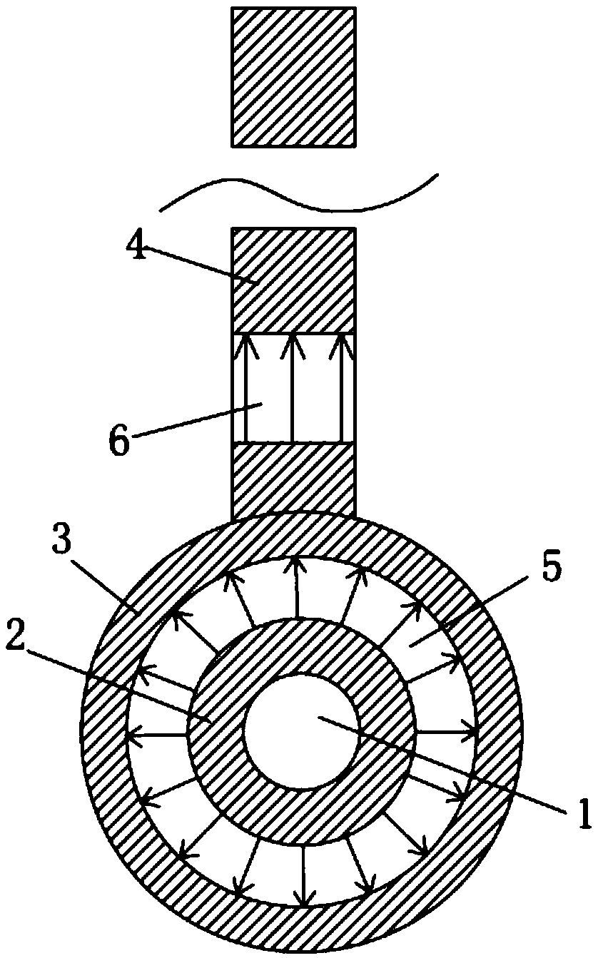
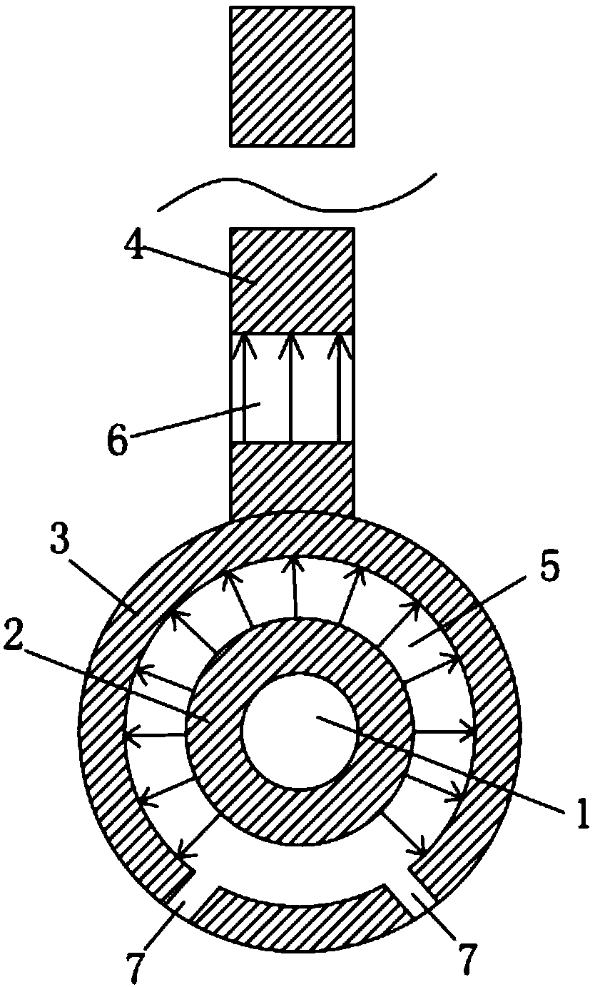
The invention discloses a method for accurately adjusting the buried resistance based on a via hole, which includes the following steps: a hole is drilled in a production board, and the hole is metalized through copper depositing and full-board electroplating, wherein the outer copper foil on the production board is a nickel-phosphorus alloy buried resistance copper foil, and the copper layer in the nickel-phosphorus alloy buried resistance copper foil is placed on the outermost side of the production board; an outer circuit is made on the production board, a hole ring is formed around the hole through alkaline etching in the making process of the outer circuit, an outer ring spaced from the hole ring is arranged at the periphery of the hole ring, the outer ring is connected with the outercircuit, and the hole ring and the outer ring are connected through the nickel-phosphorus alloy layer in the nickel-phosphorus alloy buried resistance copper foil to form an annular buried resistor;and part of the copper layer on the outer ring is removed by laser cutting, and therefore, the resistance between the hole ring and the outer ring can be accurately adjusted. By using the method of the invention, the resistance can be adjusted evenly and accurately, and the resistance precision of finished boards is improved.

Description

technical field [0001] The invention relates to the technical field of printed circuit board production, in particular to a method for accurately adjusting buried resistance based on via holes. Background technique [0002] With the continuous improvement of the integration of electronic systems, PCB embedded resistance technology, as a method to replace surface resistor patches, can save the increasingly tight surface space of PCBA, and is also more reliable than chip resistors. [0003] Nickel-phosphorus alloy buried resistance copper foil refers to sputtering or electroplating a layer of nickel-phosphorus alloy on the copper foil, forming a nickel-phosphorus alloy buried resistance plate by laminating the nickel-phosphorus alloy buried resistance copper foil with the dielectric layer or by prepreg. The phosphorus alloy buried resistance copper foil is laminated with the inner core board to form a multilayer board, in which the nickel phosphorus alloy layer is located betw...

Claims


Application Information

Patent Timeline
Patent Type & Authority Applications(China)
IPC IPC(8): H05K3/02H05K1/16
CPCH05K1/167H05K3/027H05K2203/107
Inventor 叶国俊马毅袁为群
Owner SHENZHEN SUNTAK MULTILAYER PCB
Learn More