Cone semiconductor laser

A laser and semiconductor technology, applied in the direction of semiconductor lasers, lasers, laser parts, etc., to achieve the effect of increasing the length, the beam quality is not easy to deteriorate, and the high power

Inactive Publication Date: 2019-01-04
INST OF APPLIED ELECTRONICS CHINA ACAD OF ENG PHYSICS
View PDF5 Cites 5 Cited by
  • Summary
  • Abstract
  • Description
  • Claims
  • Application Information

AI Technical Summary

Problems solved by technology

Affected by cavity surface damage and nonlinear effects, the maximum output power of the 100 μm wide chip is currently limited to about 30 W. To continue to increase the output power, it is urgent to carry out innovative research on chip design.

Method used


Image

  • Cone semiconductor laser

Examples


Embodiment

[0021] Applications in GaAs-based 980 nm lasers:

[0022] Epitaxial structure:

[0023] The substrate layer is 350 μm, the lower confinement layer is 700 nm, the waveguide layer is 2400 nm, the upper confinement layer is 700 nm, and the contact layer is 200 nm.

[0024] Chip structure:

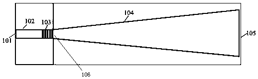
[0025] 1) Ridge area length: 1 mm;

[0026] 2) Ridge area width: 5 μm;

[0027] 3) Ridge etching depth: 1.0 𝛍m;

[0028] 4) Bragg mirror: etching depth 1.3 𝛍m, period 300 nm, logarithm 1000 pairs;

[0029] 5) Angle of cone area: 4 degrees;

[0030] 6) Length of tapered area: 4 mm;

[0031] 7) Etching depth of tapered area: 200 nm;

[0032] 8) Front cavity surface corrosion: ethylene glycol: 30% phosphoric acid: hydrogen peroxide = 20:5:1, corrosion depth 3.5 μm;

[0033] 9) Cavity surface coating: the reflection rate of the rear cavity surface is coated with high reflection film, and the reflection rate of the front cavity surface is 0.1%.


PUM


Abstract

The invention provides a tapered semiconductor laser, which comprises a ridge region and a tapered region. The seed laser near the diffraction limit is generated in the ridge region, and the seed laser enters the cone region to amplify the output. The front cavity surface of the conical region, that is, the cavity surface of one end connected with the ridge region, has no feedback laser, and the conical region unidirectionally amplifies the seed laser. The scheme can realize the unidirectional amplification of laser beam, the front cavity surface without feedback structure makes the beam quality not easy to deteriorate in the amplification process, can greatly increase the length of the conical region, can not only output high power, but also maintain the beam quality near the diffractionlimit, can achieve ultra-high brightness laser output.

Description

technical field [0001] The invention relates to the field of semiconductor laser junction design, in particular to a tapered semiconductor laser. Background technique [0002] In recent years, high-power semiconductor laser chips (LD) have developed rapidly, and are widely used as pump light sources in civil and military fields, especially as fiber laser pump sources, which have developed rapidly in recent years. As fiber lasers continue to increase the output brightness requirements of semiconductor laser pump sources, and the number of semiconductor laser chips coupled with traditional pigtail pump sources is close to the physical limit, continuing to increase output brightness can only increase the brightness of the chip. On the other hand, realizing direct output of high-brightness semiconductor lasers through high-quality and high-efficiency common-aperture beam combining is also one of the important ways to study a new generation of miniaturized, lightweight and high-p...

Claims


Application Information

Patent Timeline
Patent Type & Authority Applications(China)
IPC IPC(8): H01S5/10H01S5/125H01S5/22
CPCH01S5/1014H01S5/125H01S5/22
Inventor 周坤杜维川康俊杰李弋谭昊王昭高松信唐淳
Owner INST OF APPLIED ELECTRONICS CHINA ACAD OF ENG PHYSICS
Why Eureka
Try Eureka