Piezoelectric MEMS acceleration sensor and a preparation method thereof

An acceleration sensor and piezoelectric technology, applied in the field of micro sensors, can solve the problems of poor anti-overload capacity and low resonance frequency, and achieve the goal of increasing the bending stiffness, improving the quality factor, and improving the reliability and stability of the detection results. Effect

Active Publication Date: 2019-01-08
HEFEI UNIV OF TECH
View PDF6 Cites 7 Cited by
  • Summary
  • Abstract
  • Description
  • Claims
  • Application Information

AI Technical Summary

Problems solved by technology

[0006] In order to avoid the shortcomings of the above-mentioned prior art, the present invention provides a piezoelectric MEMS acceleration sensor and its preparation method, w

Method used


Image

  • Piezoelectric MEMS acceleration sensor and a preparation method thereof
  • Piezoelectric MEMS acceleration sensor and a preparation method thereof
  • Piezoelectric MEMS acceleration sensor and a preparation method thereof

Examples


Embodiment 1

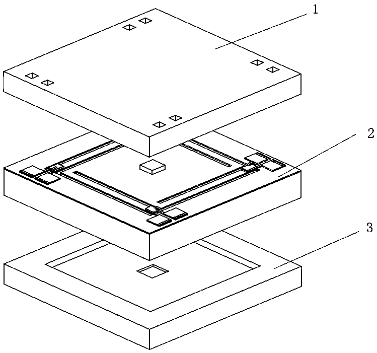
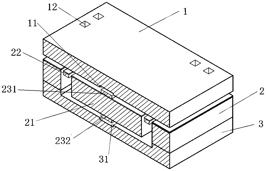
[0065] see figure 1 , figure 2 , the present embodiment provides a piezoelectric MEMS acceleration sensor, which is composed of a cover plate 1, a detection structure layer 2 and a substrate 3 connected in sequence;

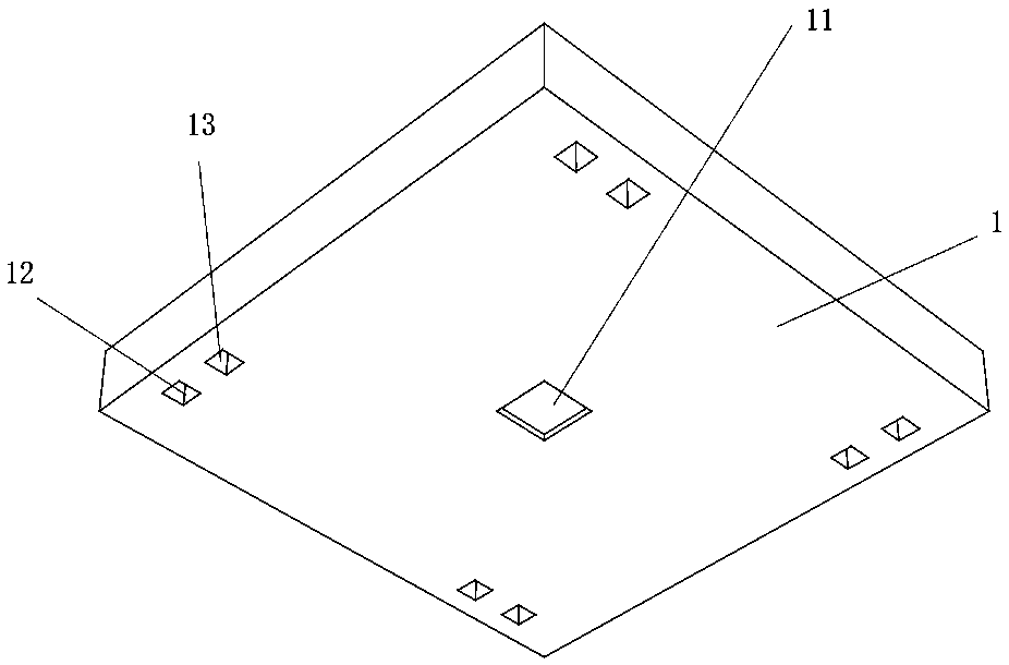
[0066] like image 3 As shown, the cover plate 1 is made on the basis of the crystal orientation N-type single-polished silicon wafer. The center of the bottom surface of the cover plate 1 is provided with an upper limit groove 11, and the four corners of the top surface of the cover plate 1 are respectively Two wire lead-out holes 12 are provided, and the wire lead-out holes 12 are set through the cover plate 1 .

[0067] like Figure 4-6 As shown, the detection structure layer 2 is made on the basis of a square double-thrown SOI silicon wafer. The detection structure layer 2 includes a square outer frame 24, a sensitive mass 21 and four L-shaped fixed beams 22 arranged in the outer frame 24, and the sensitive The outer periphery of the mass block 21 is re...

Embodiment 2

[0072] This embodiment provides a preparation method of a piezoelectric MEMS acceleration sensor, the operation steps are as follows:

[0073] Preparation: Take a double-throw SOI silicon wafer with a thickness of 351 μm and two single-throw N-type silicon wafers with crystal orientation with a thickness of 300 μm;

[0074] One-time photolithography: use the standard semiconductor cleaning process to clean the double-polished SOI silicon wafer, and place the cleaned double-polished SOI silicon wafer in an etching tank containing potassium hydroxide solution for thinning treatment, and the overall thickness of the substrate layer is reduced to 50 μm. The photoresist is spin-coated at the center of the surface of the substrate layer, developed by photolithography, and then the lower limit post 232 with a side length of 30 μm and a height of 8 μm is etched using an ICP etching (inductively coupled plasma) process, as shown in Figure 8 shown;

[0075] Secondary photolithography...


PUM

PropertyMeasurementUnit
Thicknessaaaaaaaaaa

Abstract

The invention provides a piezoelectric MEMS acceleration sensor and a preparation method thereof. The piezoelectric MEMS acceleration sensor comprises a cover plate, a detecting structure layer and abottom substrate which are successively connected. The middle part of the detecting structure layer is provided with a sensitive mass block and an L-shaped fixed supporting beam. An upper limit position column and a low limit position column are respectively arranged at that center of the upper and lower sides of the detection structure layer, and are respectively match with a cover plate and a base substrate. Furthermore a two-time silicon-silicon binding method is utilized, thereby forming the piezoelectric MEMS acceleration sensor with a closed inner part. When the whole device is subjectedto non-overload acceleration, the piezoelectric ceramic thin film is deformed and a voltage signal is generated on the surface of the device. When subjected to overload acceleration, limited by the limit structure of the outer frame, the sensitive mass only damps the gap distance of the displacement sensor system, thus playing the role of omni-directional overload protection.

Description

technical field [0001] The invention relates to the technical field of microsensors, in particular to a piezoelectric MEMS acceleration sensor and a preparation method thereof. Background technique [0002] With the development of modern industry and science and technology, industrial equipment continues to develop in the direction of complexity, intelligence, and informatization. These equipment components are sophisticated and complex, with various working modes and changing operating occasions. As the most common physical phenomenon, vibration during the operation of industrial equipment has a direct impact on the performance and health of the equipment. If the vibration exceeds the allowable range, the equipment will generate large dynamic loads and noises, resulting in high The failure rate will affect its working performance and service life. In severe cases, it will lead to early failure of components, causing huge losses or casualties. [0003] In order to effective...

Claims


Application Information

Patent Timeline
IPC IPC(8): B81B7/00B81C1/00G01H11/08
CPCB81B7/0032B81B7/0038B81C1/00261B81C1/00285G01H11/08
Inventor 许高斌王超超陈兴马渊明胡海霖
Owner HEFEI UNIV OF TECH
Why Eureka
Try Eureka