An insulated gate bipolar transistor and a preparation method thereof

A bipolar transistor and insulated gate technology, applied in semiconductor/solid-state device manufacturing, semiconductor devices, electrical components, etc., can solve problems such as band bending, low forward conduction voltage drop, increase, etc., and achieve a change in the forbidden band width , excellent device characteristics, and the effect of improving the carrier concentration distribution

Active Publication Date: 2019-01-08
UNIV OF ELECTRONICS SCI & TECH OF CHINA
View PDF3 Cites 5 Cited by
  • Summary
  • Abstract
  • Description
  • Claims
  • Application Information

AI Technical Summary

Problems solved by technology

[0008] The present invention aims at the adverse effects of the doping concentration and thickness of the charge storage layer on the breakdown voltage of the device in the prior art, and limits the compromise between the breakdown voltage of the device, the forward conduction voltage drop and the turn-off loss, and provides An insulated gate bipolar transistor with a heterojunction structure in the base region. By introducing a heterojunction into the base region, the energy band of the base region is bent, thereby forming a potential barrier to the minority carriers in the drift region. Increase the minority carrier concentration near the emitter in the drift region, improve the carrier concentration distribution in the drift region, and obtain lower forward conduction voltage drop and better forward conduction voltage drop and turn-off loss The compromise relationship avoids the adverse effect of increasing the concentration of the charge storage layer on the breakdown voltage of the device

Method used


Image

  • An insulated gate bipolar transistor and a preparation method thereof
  • An insulated gate bipolar transistor and a preparation method thereof
  • An insulated gate bipolar transistor and a preparation method thereof

Examples


Embodiment 1

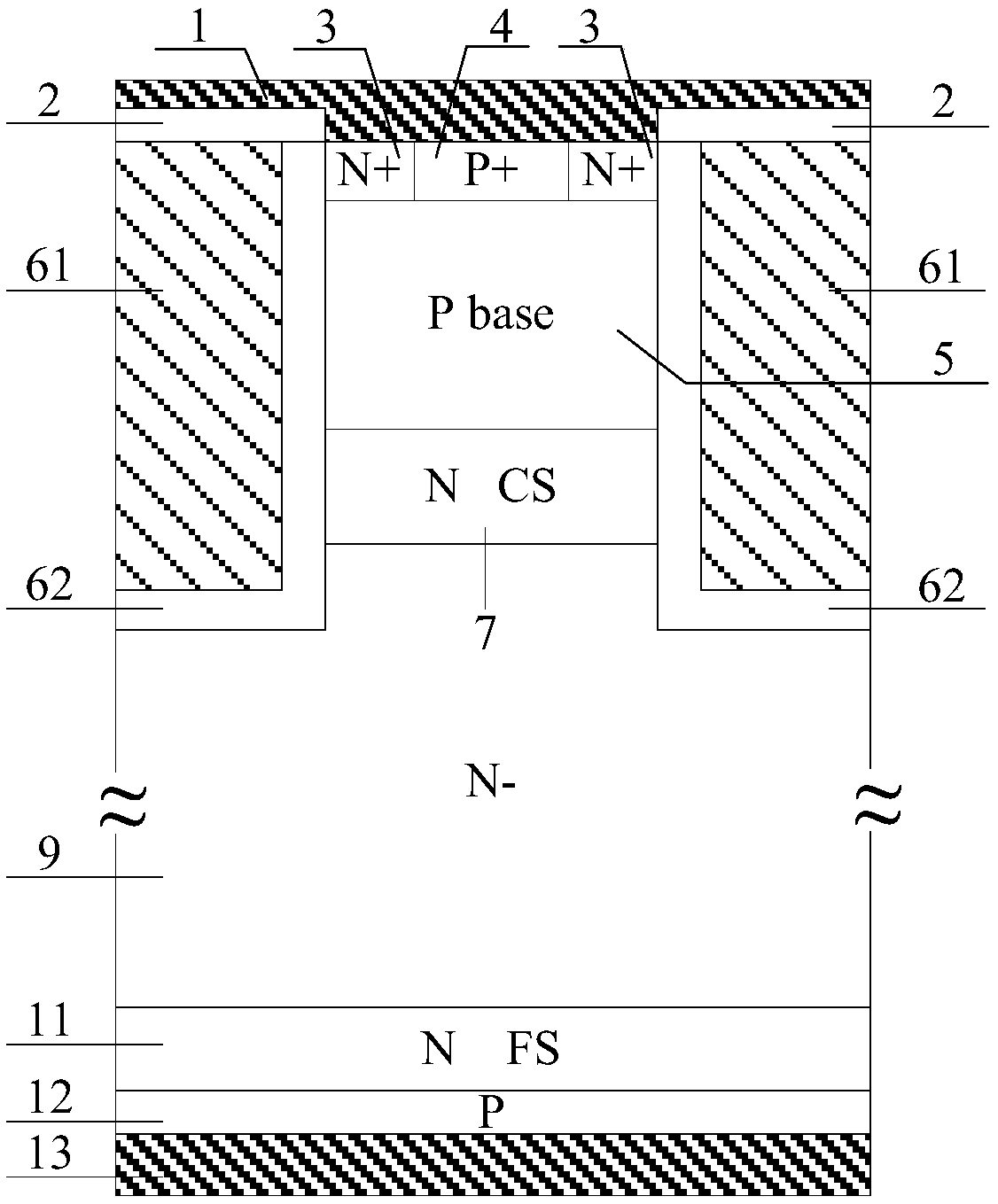
[0075] This embodiment provides a strained Si~Si 1-x Ge x Insulated gate bipolar transistors with heterojunction base regions, Figure 4 Its semi-cellular structure is shown, and its cellular structure includes: collector metal 13, P-type collector region 12, N-type drift region 9, P-type base region 5, P+ emitter region 4, N+ emitter region 3, gate structure and the emitter metal 1; the collector metal 13 is arranged on the back of the P-type collector region 12; the N-type drift region 9 is arranged on the front of the P-type collector region 12; the P-type base region 5 is arranged on the side of the N-type drift region 9 Top layer; P+ emitter region 4 and the N+ emitter region 3 that is in contact with both sides of P+ emitter region 4 are arranged side by side on the top layer of P-type base region 5; the gate structure includes gate electrode 61 and gate dielectric layer 62, and gate electrode 61 passes gate The dielectric layer 62 is in contact with the N+ emitter reg...

Embodiment 2

[0081] This embodiment provides a strained Si~Si 1-x Ge x Insulated gate bipolar transistors with heterojunction base regions, Figure 11 Its semi-cellular structure is shown. In this embodiment, except in P-type Si 1-x Ge x A P-type Si layer 53 is added on the lower surface of the layer 52 to form a double potential barrier. The junction depths of the P-type Si base region 51 and the P-type Si layer 53 are both 1 μm, and the rest of the structure is the same as that of Embodiment 1.

[0082] In this embodiment, the P-type Si 1-x Ge x A P-type Si layer 53 is added to the lower surface of the base region 52, thereby introducing a heterojunction hole barrier, further improving the conductance modulation effect of the device, thereby reducing the forward conduction voltage drop and conduction loss of the device, and improving The trade-off relationship between the turn-off loss and the forward conduction voltage drop is shown.

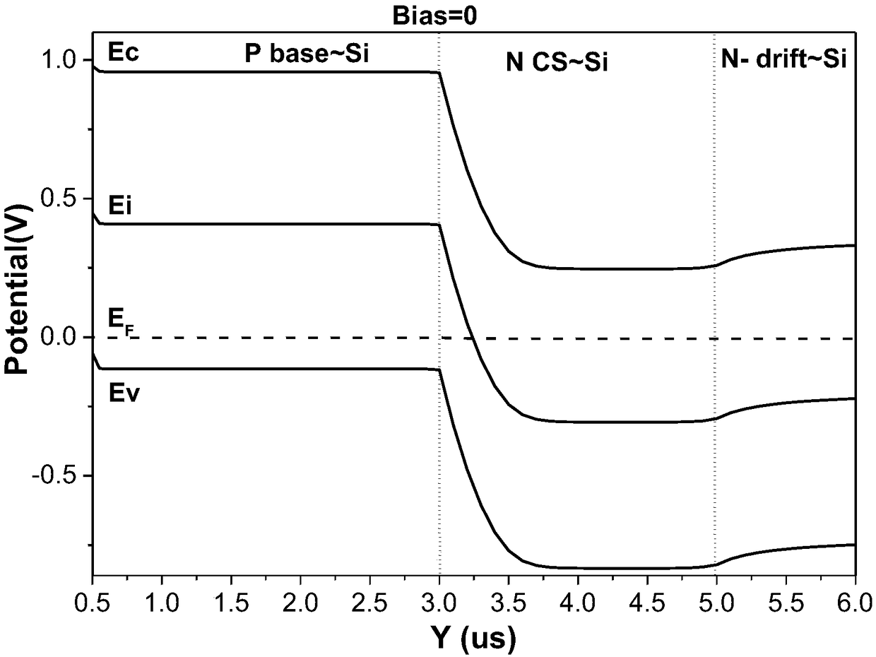
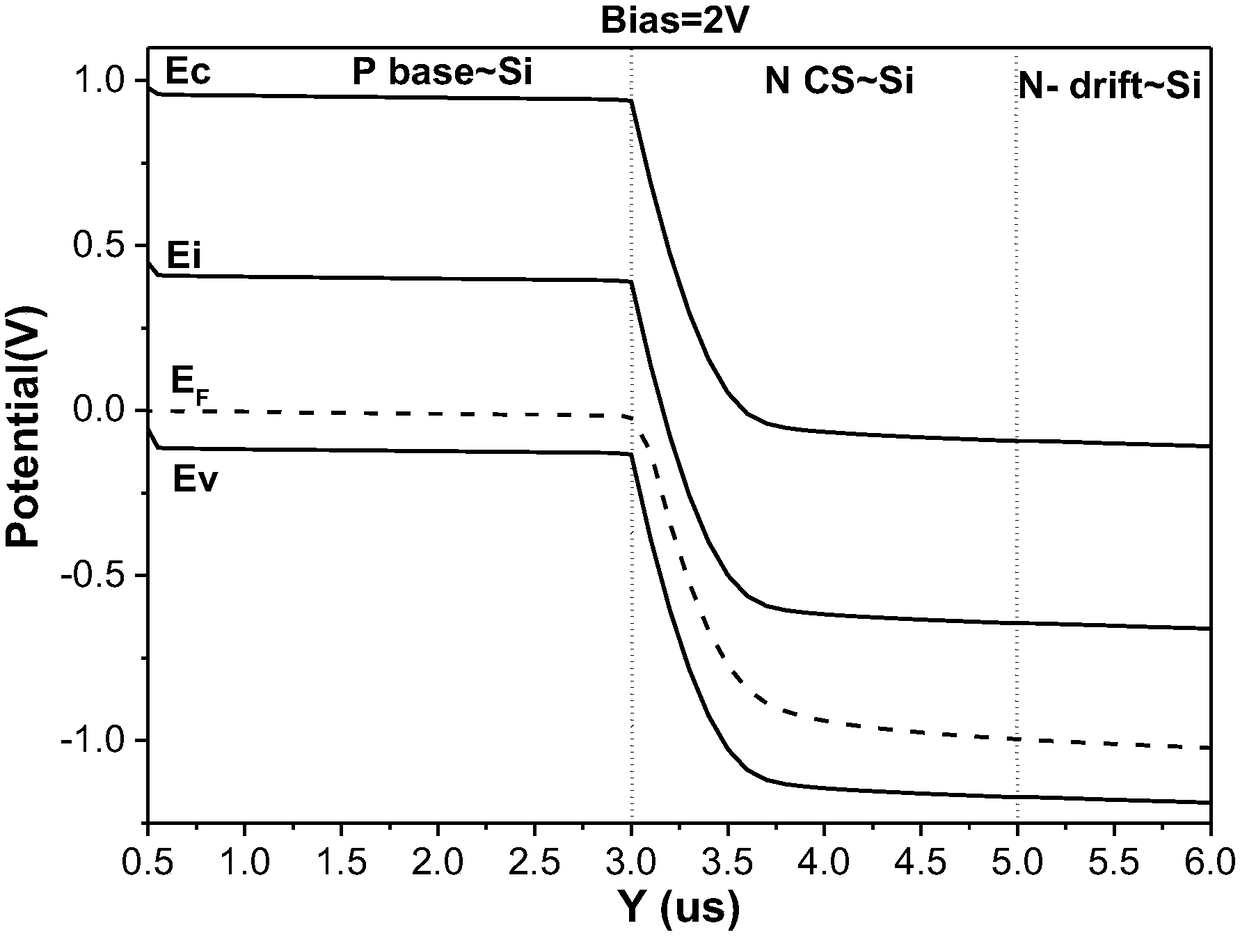
[0083] Figure 12 with 13 Respectively Si~...

Embodiment 3

[0087] This embodiment provides a strained Si~Si 1-x Ge x Insulated gate bipolar transistors with heterojunction base regions, Figure 16 Its semi-cellular structure is shown. In this embodiment, except that an N-type charge storage layer 7 with a junction depth of 2 μm is introduced under the P-type base region 5 , other structures are the same as those in Embodiment 2.

[0088] In this embodiment, the hole barrier is introduced on the side of the N-drift region 9 close to the emitter by introducing the N-type charge storage layer 7, thereby further improving the conductance modulation effect of the device and reducing the forward conduction voltage drop and conduction of the device. Loss, while improving the trade-off relationship between turn-off loss and forward voltage drop.


PUM


Abstract

The invention relates to an insulated gate bipolar transistor and a preparation method thereof, belonging to the technical field of power semiconductors. On the basis of the traditional charge storagetype IGBT device structure, A heterojunction structure is formed in the base region, thereby forming a potential barrier that prevents minority carriers in the drift region from flowing into the baseregion, thereby greatly increasing the minority carrier concentration near the emitter side in the drift region, The carrier concentration distribution in drift region is improved and the conductivity modulation effect of IGBT is enhanced, which reduces the forward conduction voltage drop Vceon and optimizes the tradeoff between the forward conduction voltage drop Vceon and the shutdown loss Eoffof IGBT. It overcomes the shortcoming that the traditional charge storage layer reduces Vceon and breakdown voltage at the same time. Moreover, the device performance can be further optimized by adjusting the combination of semiconductor materials with different forbidden band widths to form heterojunction structures.

Description

technical field [0001] The invention belongs to the technical field of power semiconductor devices, and in particular relates to an insulated gate bipolar transistor and a preparation method thereof. Background technique [0002] IGBT is a device composed of MOSFET (input stage) and PNP transistor (output stage). It not only has the characteristics of easy driving, low input impedance and fast switching speed of MOSFET devices, but also has the on-state current density of bipolar devices. Large, low conduction voltage, low loss, and good stability. Based on these excellent device characteristics, IGBT has become a mainstream power device widely used in medium and high voltage fields in recent years, such as high-speed rail, electric vehicles, motor drives, grid-connected technology, energy storage power stations, AC / DA conversion and frequency conversion speed regulation and other fields . The use of IGBT for power conversion can improve the efficiency and quality of power...

Claims


Application Information

Patent Timeline
Patent Type & Authority Applications(China)
IPC IPC(8): H01L29/739H01L29/423H01L29/10H01L21/331
CPCH01L29/1095H01L29/4232H01L29/66348H01L29/7397H01L29/7398
Inventor 张金平赵倩王康刘竞秀李泽宏张波
Owner UNIV OF ELECTRONICS SCI & TECH OF CHINA
Why Eureka
Try Eureka