A planar insulated gate bipolar transistor and a preparation method thereof

A bipolar transistor, insulated gate technology, used in transistors, semiconductor/solid-state device manufacturing, semiconductor devices, etc., can solve the compromise of increasing forward voltage drop, increasing device drift region, forward voltage drop and turn-off loss characteristics deterioration and other problems, to achieve the effect of reducing the on-voltage drop, optimizing the turn-off loss, and enhancing the conductance modulation effect

Active Publication Date: 2019-01-08
UNIV OF ELECTRONICS SCI & TECH OF CHINA
View PDF5 Cites 6 Cited by
  • Summary
  • Abstract
  • Description
  • Claims
  • Application Information

AI Technical Summary

Problems solved by technology

Therefore, in order to maintain a certain blocking capability of the device in practical applications, technicians have to increase the thickness of the drift region of the device, which instead increases the forward voltage drop and deteriorates the compromise between forward voltage drop and turn-off loss.

Method used


Image

  • A planar insulated gate bipolar transistor and a preparation method thereof
  • A planar insulated gate bipolar transistor and a preparation method thereof
  • A planar insulated gate bipolar transistor and a preparation method thereof

Examples


Embodiment 1

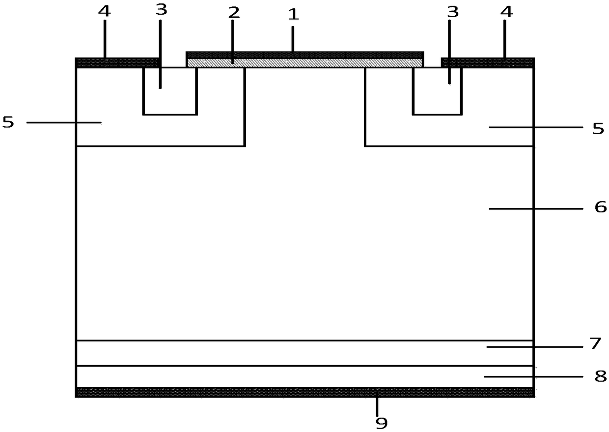
[0044] This embodiment provides a silicon carbide planar insulated gate bipolar transistor, including: a metallized collector 9, a P-type collector region 8, an N-type electric field stop layer 7, an N-drift region 6, and a P-type base region 5 , N+ emitter region 3, planar gate structure and emitter metal 4; metallized collector electrode 9 is located on the back of P-type collector region 8, N-type electric field stop layer 7 is located on the front of P-type collector region 8, N-type electric field stop Layer 7 is located on the front of the N-drift region 6; the P-type base region 5 is located on both sides of the top layer of the N-drift region 6; the N+ emitter region 3 is located on the top layer of the P-type base region 5, and is separated from the N-drift region 6 P-type base region 5; the upper surface of the P-type base region 5 between the N+ emitter regions 3 on both sides and part of the upper surface of the N+ emitter region 3 have a planar gate structure; on t...

Embodiment 2

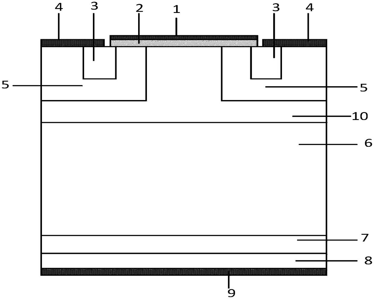
[0050] This embodiment provides a silicon carbide planar insulated gate bipolar silicon carbide transistor, the cell structure of which is as follows Figure 4 As shown, on the basis of Example 1, the P-type silicon layer 11 can also extend to the lower P-type base region 5 to form a trench structure, and the P-type silicon layer 11 is connected to the P-type silicon layer at the bottom and side walls of the trench. The P-type base region 5 and the N-type emitter region 3 form a heterojunction; the trench depth of the P-type silicon layer 11 may be the same as that of the N+ emitter region 3 or may be different.

[0051] Compared with Embodiment 1, this embodiment reduces the parasitic resistance formed in the P-type base region 5, reduces the voltage drop formed by the hole current in the P-type base region 5, and further suppresses the possible dynamic latch of the device. lock, which improves the high current shutdown capability of the device.

Embodiment 3

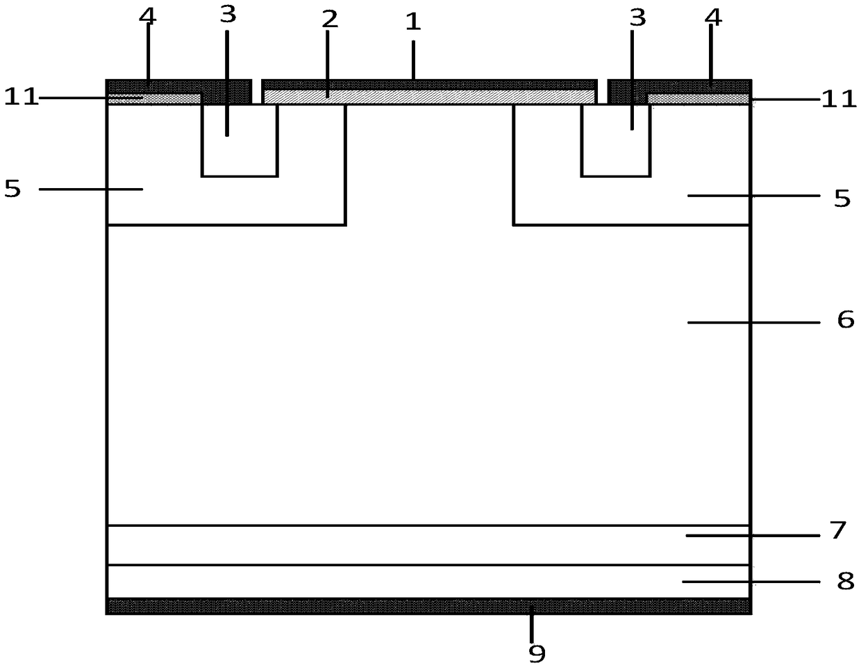
[0053] This embodiment provides a silicon carbide planar insulated gate bipolar silicon carbide transistor, the cell structure of which is as follows Figure 5 As shown, on the basis of Embodiment 2, the lower part of the P-type silicon layer 11 may also be a heavily doped P-type contact region 12, and the concentration of the P-type contact region 12 is greater than that of the P-type base region 5. concentration; the P-type silicon layer 11 and the P-type contact region 12 form a heterojunction.

[0054] Compared with Example 2, the concentration of the heavily doped P-type contact region 12 is much higher than that of the P-type base region 5, thereby forming a higher hole barrier, which can further increase the potential of the P-type base region and enhance the conductance modulation effect.


PUM


Abstract

The invention relates to a planar insulated gate bipolar transistor and a preparation method thereof, belonging to the technical field of power semiconductors. A semiconductor layer or Schottky contact metal having a relatively small band gap is introduced into the upper surface of the base region of the device adjacent to the outer side of the emitter region, By using heterojunction or Schottky contact as minority carrier barrier to enhance the conductivity modulation effect, the conduction voltage drop is reduced and the tradeoff between forward voltage drop and turn-off loss is optimized. As the heterojunction or Schottky contact introduced by the invention can replace the CS layer functionally, the electric field strength of the PN junction formed in the base region and the drift region is reduced to improve the breakdown voltage of the device; And the electric field intensity of the gate oxide layer is below the safe value (3MV/cm), so the reliability of the gate oxide layer is ensured. In addition, the fabrication process of the device is simple and controllable, and the device has strong compatibility with the existing process.

Description

technical field [0001] The invention belongs to the technical field of power semiconductors, and in particular relates to a planar insulated gate bipolar transistor and a preparation method thereof. Background technique [0002] Insulated Gate Bipolar Transistor (IGBT) is a bipolar device controlled by an insulated gate. The higher the non-equilibrium carrier concentration in the body, the more significant the conductance modulation effect and the higher the current density. figure 1 It shows a semi-cellular structure of a traditional trench type IGBT device. When the device is in forward conduction, due to the extraction of minority carriers by the reverse-biased PN junction formed by the base region 5 and the drift region 6, the conductance modulation effect is not significant. Significantly, the forward voltage drop is too large, and the compromise characteristics cannot be improved. Such as figure 2 As shown, the conductance modulation effect in the drift region is en...

Claims


Application Information

Patent Timeline
Patent Type & Authority Applications(China)
IPC IPC(8): H01L29/739H01L29/10H01L29/08H01L29/06H01L21/331
CPCH01L29/0623H01L29/0817H01L29/1095H01L29/66333H01L29/7398
Inventor 张金平罗君轶赵阳刘竞秀李泽宏张波
Owner UNIV OF ELECTRONICS SCI & TECH OF CHINA
Why Eureka
Try Eureka