A method for manufacture a double buffer lay perovskite solar cell
A technology of solar cells and manufacturing methods, which can be applied in the direction of final product manufacturing, sustainable manufacturing/processing, semiconductor/solid-state device manufacturing, etc., and can solve problems such as backward conversion efficiency
- Summary
- Abstract
- Description
- Claims
- Application Information
AI Technical Summary
Problems solved by technology
Method used
Image
Examples
Embodiment 1
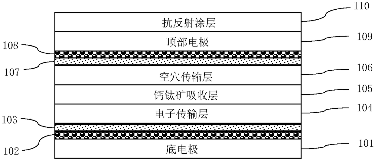
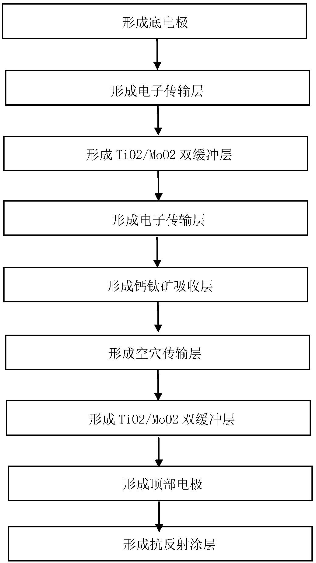
[0028] The FTO transparent conductive glass was ultrasonically cleaned with acetone, ethanol, and deionized water in sequence, and then treated with ultraviolet and ozone to obtain a clean 100 nm transparent conductive glass as the bottom electrode 101 . Use the sol-gel method to spin-coat on the FTO transparent conductive glass substrate to form nano-titanium dioxide particles 102 with a thickness of 20nm, then dry at room temperature to remove excess solvent, and then form a layer of 30nm molybdenum dioxide on it by hydrothermal method layer 103, and slowly raise the temperature to 60°C for drying treatment to form nano-TiO 2 / MoO 2 The buffer layer.
[0029] A layer of TiO electron transport layer 104 with a thickness of 80 nm was formed on the buffer layer, and then a perovskite thin film was spin-coated on the electron transport layer, and the film was placed in a vacuum chamber for 3 seconds to promote perovskite by removing residual solvent. Ore nucleation, spin coati...
Embodiment 2
[0033] The ITO transparent conductive glass was ultrasonically cleaned with acetone, ethanol, and deionized water in sequence, and then treated with ultraviolet and ozone to obtain a clean 100 nm transparent conductive glass as the bottom electrode 101 . Use the sol-gel method to spin-coat on the ITO transparent conductive glass substrate to form nano-titanium dioxide particles 102 with a thickness of 20nm, then dry at room temperature to remove excess solvent, and then form a layer of 30nm molybdenum dioxide on it by hydrothermal method layer 103, and slowly raise the temperature to 60°C for drying treatment to form nano-TiO 2 / MoO 2 The buffer layer.
[0034] A 20nm ZnO electron transport layer 104 is formed on the buffer layer, followed by spin-coating a perovskite thin film on the electron transport layer, and placing the film in a vacuum chamber for 3 seconds to promote the formation of perovskite by removing residual solvent. The core is spin-coated in ambient air; spi...
PUM
 Abstract
Description
Claims
Application Information

