A kind of oled display substrate and its manufacturing method, oled display device

A technology for display substrates and substrate substrates, which is applied in semiconductor/solid-state device manufacturing, semiconductor devices, electrical components, etc., and can solve the problems of large volume occupied by OLED displays and the inability to meet the thinning and thinning of OLED displays.

Active Publication Date: 2020-11-03
BOE TECH GRP CO LTD +1
View PDF6 Cites 0 Cited by
  • Summary
  • Abstract
  • Description
  • Claims
  • Application Information

AI Technical Summary

Problems solved by technology

[0003] The piezoelectric driver is used in the OLED display to realize the screen sound function, and the ultrasonic sensor is used to realize the fingerprint recognition function. The inventors have found that if the OLED display wants to realize the screen sound function and the fingerprint recognition function at the same time, it is necessary to set the piezoelectric driver and the ultrasonic sensor at the same time, so that OLED displays occupy a large volume, which cannot meet the needs of thinner and lighter OLED displays

Method used


Image

  • A kind of oled display substrate and its manufacturing method, oled display device
  • A kind of oled display substrate and its manufacturing method, oled display device
  • A kind of oled display substrate and its manufacturing method, oled display device

Examples


Embodiment 1

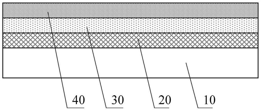
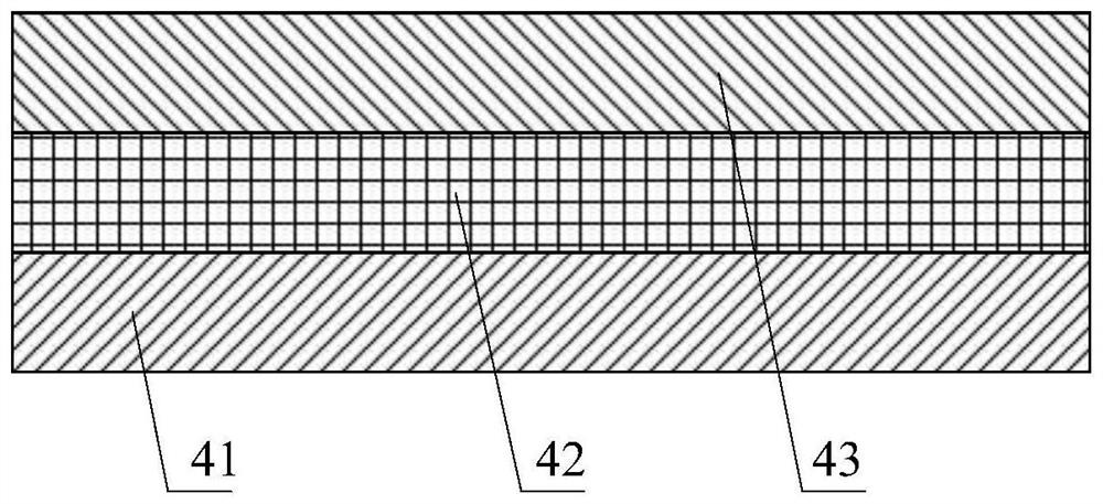
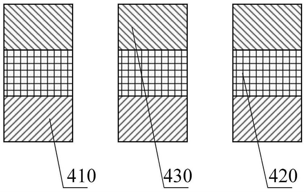
[0072] figure 1 Schematic structure of the OLED display substrate provided for the embodiment of the present invention Figure 1 ,Such as figure 1 As shown, the embodiment of the present invention provides an OLED display substrate, including: a base substrate 10, an OLED device layer 20 disposed on the base substrate 10, and an encapsulation layer 30 for encapsulating the OLED device layer 20, and the OLED display substrate also It includes: a piezoelectric functional layer 40 .

[0073] Specifically, the piezoelectric functional layer 40 is disposed on a side of the encapsulation layer 30 away from the base substrate 10 , and is used for generating mechanical vibrations under the action of electrical signals to generate ultrasonic waves or audible sound waves.

[0074] Optionally, the manufacturing material of the base substrate 10 includes: glass, plastic, quartz, or polyimide, etc., which is not limited in this embodiment of the present invention.

[0075] Specifically,...

Embodiment 2

[0122] Based on the inventive concepts of the above embodiments, the embodiments of the present invention also provide a method for manufacturing an OLED display substrate, Figure 14 A flow chart of a method for manufacturing an OLED display substrate provided in an embodiment of the present invention, such as Figure 14 As shown, the manufacturing method of the OLED display substrate provided by the embodiment of the present invention specifically includes the following steps:

[0123] Step 100, providing a base substrate.

[0124] Optionally, the manufacturing material of the base substrate includes: glass, plastic, quartz, or polyimide, etc., which is not limited in this embodiment of the present invention.

[0125] Step 200, forming an OLED device layer on the base substrate.

[0126] Specifically, the OLED device layer includes: a thin film transistor and an anode, a light-emitting layer, and a cathode disposed on the thin film transistor, wherein the thin film transis...

Embodiment 3

[0172] Based on the inventive concepts of the above embodiments, the embodiments of the present invention further provide an OLED display device, including: an OLED display substrate.

[0173] Wherein, the OLED display substrate is the OLED display substrate provided in Embodiment 1, and its realization principle and realization effect are similar, and will not be repeated here.

[0174] Specifically, the OLED display device may be any product or component with a display function such as an OLED panel, a mobile phone, a tablet computer, a television set, a monitor, a notebook computer, a digital photo frame, a navigator, and the like.

[0175] The drawings of the embodiments of the present invention only relate to the structures involved in the embodiments of the present invention, and other structures may refer to common designs.

[0176] In the drawings used to describe embodiments of the present invention, the thickness and size of layers or microstructures are exaggerated ...


PUM


Abstract

Embodiments of the present invention provide an OLED display substrate, a manufacturing method thereof, and an OLED display device, wherein the OLED display substrate includes: a base substrate, an OLED device layer disposed on the base substrate, and an encapsulation layer for encapsulating the OLED device layer , further comprising: a piezoelectric functional layer; the piezoelectric functional layer is disposed on a side of the packaging layer away from the base substrate, and is used to generate mechanical vibration under the action of an electrical signal to generate ultrasonic waves or audible sound waves. In the embodiment of the present invention, a piezoelectric functional layer is provided in the OLED display substrate, and ultrasonic waves and audible sound waves are generated through its mechanical vibration, and the screen sound and fingerprint recognition functions are realized by using the same structure, which reduces the volume occupied by the OLED display and satisfies the requirements of the OLED display. Thinning needs.

Description

technical field [0001] Embodiments of the present invention relate to the field of display technology, and in particular to an OLED display substrate, a manufacturing method thereof, and an OLED display device. Background technique [0002] Organic light-emitting diode (Organic Light-Emitting Device, referred to as OLED) display is a display that is different from traditional liquid crystal display (Liquid Crystal Display, referred to as LCD) with active light emission, good temperature characteristics, low power consumption, fast response, and The advantages of bending, ultra-thin and low cost. Therefore, it has become one of the important development discoveries of the new generation display device, and has received more and more attention. [0003] The piezoelectric driver is used in the OLED display to realize the screen sound function, and the ultrasonic sensor is used to realize the fingerprint recognition function. The inventors have found that if the OLED display wa...

Claims


Application Information

Patent Timeline
Patent Type & Authority Patents(China)
IPC IPC(8): H01L27/32H01L51/56
CPCH10K59/00H10K59/1201H10K71/00
Inventor 马国强柴媛媛孙阔汪杨鹏陈鹏唐国强代伟男
Owner BOE TECH GRP CO LTD
Why Eureka
Try Eureka