Semiconductor device and manufacturing method thereof

一种制造方法、半导体的技术,应用在半导体/固态器件制造、半导体器件、电气元件等方向,能够解决元件效能影响、工艺困难度高、工艺步骤繁杂等问题,达到降低生产成本、工艺步骤简单、避免工艺不稳定的效果

Active Publication Date: 2019-02-05
NUVOTON
View PDF6 Cites 0 Cited by
  • Summary
  • Abstract
  • Description
  • Claims
  • Application Information

AI Technical Summary

Problems solved by technology

[0003] However, in the ion implantation process, dopants need to be accurately implanted into the predetermined area, so the process is difficult and the process steps are relatively complicated
In addition, after the implantation of N-type dopants and P-type dopants, N-type dopants and P-type dopants tend to diffuse in the subsequent high-temperature process, which affects device performance

Method used


Image

  • Semiconductor device and manufacturing method thereof
  • Semiconductor device and manufacturing method thereof
  • Semiconductor device and manufacturing method thereof

Examples


Embodiment Construction

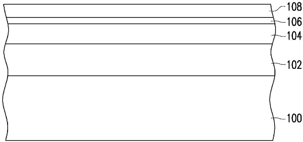
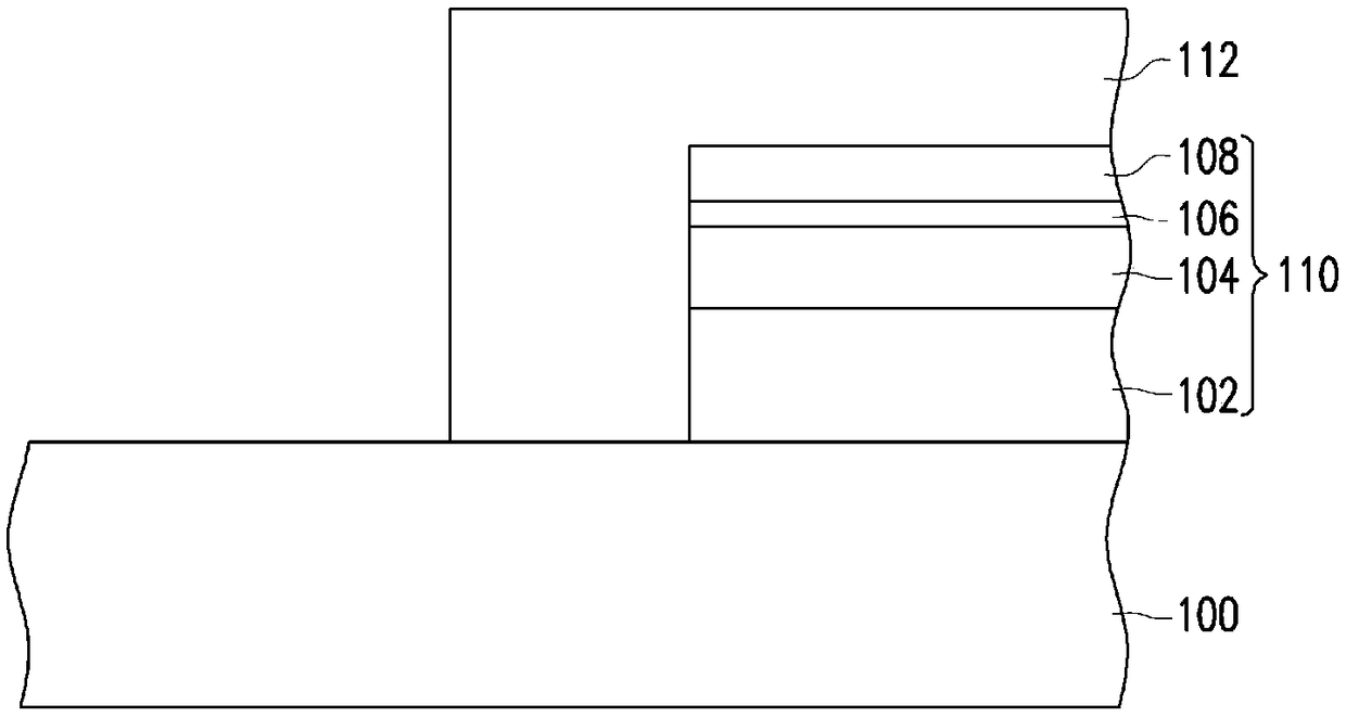
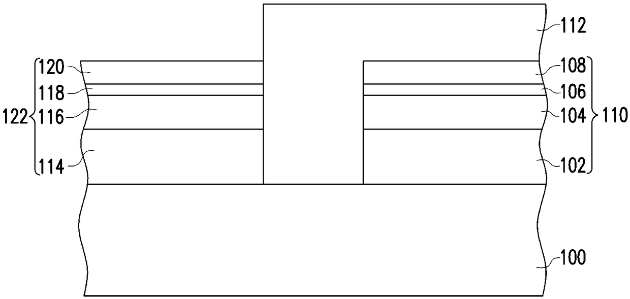
[0035] Figure 1A to Figure 1D It is a schematic cross-sectional view of a semiconductor device according to an embodiment of the present invention. First, please refer to Figure 1A , providing a substrate 100. The substrate 100 is, for example, a silicon substrate, a SiC substrate, a sapphire substrate or a GaN substrate. Then, a buffer layer 102 is selectively formed on the substrate 100 . The material of the buffer layer 102 is, for example, GaN, AlGaN or AlN. In addition, the buffer layer 102 can be doped with C or Fe to increase the resistance. The buffer layer 102 is formed by, for example, performing an epitaxial growth process. The thickness of the buffer layer 102 is, for example, between 1 um and 4 um. Next, a GaN channel layer 104 is formed on the buffer layer 102 . The GaN channel layer 104 is formed by, for example, metal organic chemical vapor deposition (MOCVD), molecular beam epitaxy (MBE) and other deposition processes. In this embodiment, the formed G...


PUM


Abstract

A semiconductor device and a manufacturing method thereof are provided. The semiconductor device includes a first stacked structure, a second stacked structure, an isolation layer and a gate. The first stacked structure is disposed on a substrate, and includes a first GaN channel layer disposed on the substrate and having an N crystal phase and a first barrier layer disposed on the first GaN channel layer. The second stacked structure is disposed on the substrate, and includes a second GaN channel layer disposed on the substrate and having a Ga crystal phase and a second barrier layer disposedon the second GaN channel layer. The isolation layer is disposed between the first stacked structure and the second stacked structure. The gate is disposed on the first stacked structure, the isolation layer and the second stacked structure. The invention can make the process steps simple, and can reduce the difficulty of manufacture and reduce the production cost.

Description

technical field [0001] The present invention relates to a semiconductor element, and in particular to a semiconductor element with an N-type channel and a P-type channel and a manufacturing method thereof. Background technique [0002] For GaN-based semiconductor elements, due to their advantages of high electron mobility, high voltage resistance, low channel resistance, and fast switching, they have gradually been widely used. In a GaN-based semiconductor element (such as a complementary metal oxide semiconductor transistor (CMOS)) with an N-type channel and a P-type channel, the N-type dopant and the P-type dopant are usually implanted separately by ion implantation. into different channel layers to form N-type channels and P-type channels. [0003] However, during the ion implantation process, dopants need to be accurately implanted into predetermined regions, so the process is relatively difficult and the process steps are complicated. In addition, after the N-type dop...

Claims


Application Information

Patent Timeline
Patent Type & Authority Applications(China)
IPC IPC(8): H01L27/092H01L21/8252
CPCH01L21/8252H01L27/092H01L21/823807H01L27/0605H01L29/045H01L29/2003H01L29/66462H01L29/7786H01L21/0254H01L29/0642H01L29/1025H01L29/66446
Inventor 陈智伟林恒光
Owner NUVOTON
Why Eureka
Try Eureka