
Ultrathin silicon nitride micro-gate chip

A technology of silicon nitride micro-gate and silicon nitride layer, which is applied in the manufacture of electrical components, electrical solid-state devices, semiconductor/solid-state devices, etc., and can solve problems such as large background noise of copper grid, large background noise, and difficult atomic-level imaging , to achieve the effects of overcoming image damage, high image signal-to-noise ratio, and wide application range

Inactive Publication Date: 2019-02-12
厦门芯极科技有限公司
View PDF5 Cites 1 Cited by
  • Summary
  • Abstract
  • Description
  • Claims
  • Application Information

AI Technical Summary

Problems solved by technology

[0003] At present, the chip carriers used for the characterization of solid-state nanomaterials are mainly carbon support films, copper mesh micro-grid support films, ultra-thin carbon support films, etc. The background noise of copper mesh is large, and it is difficult to be used for imaging liquid and gas samples.
The carbon film usually has a thickness of more than ten nanometers, and the thickness of the carbon film on the ultra-thin carbon film is 3-5nm, and the carbon film will produce a large background noise in the transmission electron microscope mode. For nanoparticles of 2-3nm, or Smaller clusters, quantum dots and other structures are difficult to achieve atomic-level imaging. At the same time, when the magnification is large, the electron beam is strong, and the carbon film will be broken by the electron beam, making it impossible to take atomic-level photos. This has also become a nanomaterial. A pressing problem in atomic-scale imaging

Method used


Image

  • Ultrathin silicon nitride micro-gate chip
  • Ultrathin silicon nitride micro-gate chip
  • Ultrathin silicon nitride micro-gate chip

Examples


Embodiment 1

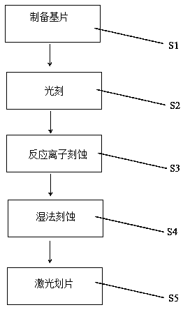
[0029] S1) Preparation of the substrate: Prepare a silicon substrate with silicon nitride layers on both sides, the size of the silicon substrate is 3mm*3mm, the thickness is 100μm, and the thickness of the silicon nitride layer is 5nm;

[0030] S2) Lithography: Expose in a UV lithography machine for 15 seconds, transfer the square porous window pattern from the photolithography mask to the side of the silicon substrate of S1), then place the silicon substrate in a positive gel developer for 30 seconds, and then Clean the surface with deionized water;

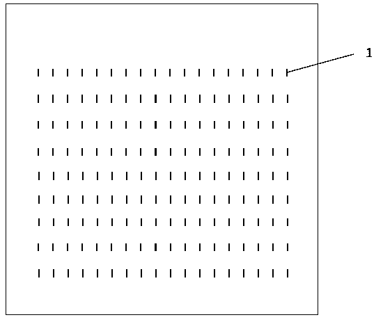
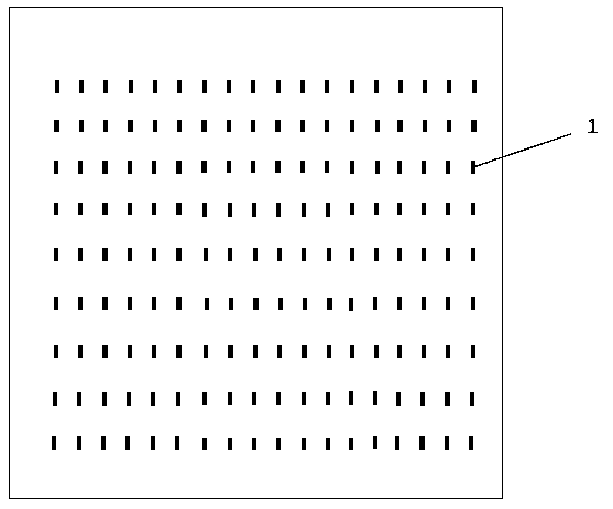
[0031] S3) Reactive ion etching: multiple viewing windows 1 are etched on the silicon nitride layer on the other side of the silicon substrate produced in S2). The viewing window 1 is 5μm*50μm in size, and then the silicon substrate is placed Into SF 6 Soak in medium for 90 seconds, with window 1 facing upward, and finally use SF 6 Rinse, wash away the photoresist;

[0032] S4) Wet etching: Put the silicon substrate produced in S3) i...

Embodiment 2

[0035] S1) Preparation of the substrate: prepare a silicon substrate with silicon nitride layers on both sides, the size of the silicon substrate is 3mm*3mm, the thickness is 100μm, and the thickness of the silicon nitride layer is 25nm;

[0036] S2) Photolithography: Expose in a UV lithography machine for 18s, transfer the square porous window pattern from the photolithography mask to the side of the silicon substrate of S1), then place the silicon substrate in a positive rubber developer for 40s, and then Clean the surface with deionized water;

[0037] S3) Reactive ion etching: multiple viewing windows 1 are etched on the silicon nitride layer on the other side of the silicon substrate produced in S2). The viewing window 1 is 15μm*50μm in size, and then the silicon substrate is placed Enter CHF 3 O 2 Soak in medium for 100s, with window 1 facing up, and finally use CHF 3 O 2 Rinse, wash away the photoresist;

[0038] S4) Wet etching, put the silicon substrate produced in S3) into...

Embodiment 3

[0041] S1) Preparation of the substrate: prepare a silicon substrate with silicon nitride layers on both sides, the size of the silicon substrate is 3mm*3mm, the thickness is 100μm, and the thickness of the silicon nitride layer is 50nm;

[0042] S2) Lithography: Expose in a UV lithography machine for 23 seconds, transfer the square porous window pattern from the photolithography mask to the side of the silicon substrate of S1), then place the silicon substrate in a positive rubber developer for 50 seconds, and then Clean the surface with deionized water;

[0043] S3) Reactive ion etching: multiple viewing windows 1 are etched on the silicon nitride layer on the back of the silicon substrate produced in S2). The viewing window 1 is 30μm*50μm in size, and then the silicon substrate is placed SF 6 Soak in medium for 110s, with window 1 facing up, and finally use SF 6 Rinse, wash away the photoresist;

[0044] S4) Wet etching: Put the silicon substrate produced in S3) into a 9.8mol / L p...


PUM

PropertyMeasurementUnit
Thicknessaaaaaaaaaa
Thicknessaaaaaaaaaa

Abstract

The invention provides an ultrathin silicon nitride micro-gate chip. A manufacturing process comprises the steps of S1 preparing a substrate, to be specific, preparing a silicon substrate with siliconoxide layers on both sides; S2 photoetching, to be specific, photoetching with an ultraviolet photoetching unit, developing, and washing with deionized water; S3 performing reactive ion etching, to be specific, etching a window, flushing with a cleaning agent, and flushing away photoresist; S4 performing wet etching, to be specific, performing wet etching with potassium hydroxide solution, and flushing with deionized water; S5, performing laser dividing, to be specific, dividing into independent chips. The manufacturing process is suitable for manufacturing ultrathin silicon nitride micro-gate chips 100 mu m in thickness; the ultrathin silicon nitride micro-gate chip manufactured via the manufacturing process uses silicon nitride as support film, silicon nitride is 5-50 nm in thickness, imaging effect is effectively improved, background noise is reduced, and the applicable range of the ultrathin silicon nitride micro-gate chip is widened; the ultrathin silicon nitride micro-gate chiphas higher controllability for measuring liquid, gas and solid samples.

Description

Technical field [0001] The invention belongs to the field of in-situ electron microscopy characterization, and specifically relates to an ultrathin silicon nitride microgate chip. Background technique [0002] Transmission Electron Microscope (TEM) is a powerful modern material characterization method, used for solid nanomaterials with spatial resolution up to atomic level. Due to the rapid development of MEMS technology, MEMS chips can integrate more and more physical and chemical functions, and the chips can be patterned, functional, and small in size. They can be combined with TEM sample rods through a series of structural and processing designs. It can be made into a sample carrier that can be used for transmission electron microscopy imaging, and can be used for high-resolution imaging of nanomaterials, especially clusters, quantum dots and other small nanomaterials. [0003] Currently, the chip carriers used for the characterization of solid-state nanomaterials are mainly ca...

Claims


Application Information

Patent Timeline
IPC IPC(8): H01L21/027H01L21/311H01L21/306H01L23/31
CPCH01L21/0274H01L21/30604H01L21/31116H01L23/3171
Inventor 邱晓滨欧阳亮
Owner 厦门芯极科技有限公司
Learn More