Metal grid high-power vertical cavity surface emitting laser
A vertical cavity surface emission, metal grid technology, applied in lasers, laser parts, semiconductor lasers, etc., can solve the problem of uneven distribution of laser current density, save volume and cost, reduce cost, and improve power density. Effect
- Summary
- Abstract
- Description
- Claims
- Application Information
AI Technical Summary
Problems solved by technology
Method used
Image
Examples
Embodiment 1
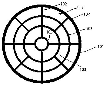
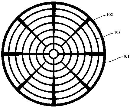
[0044] Such as Figure 1~Figure 5 As shown, this embodiment provides a metal grid high-power vertical cavity surface emitting laser. After research and analysis, the existing vertical cavity surface emitting laser with a ring-shaped upper electrode structure, when the current is injected, the current will mainly concentrate on the emission The edge area of the hole 100, while the current in the middle area of the emission hole 100 is small or even has no current, the current distribution in the edge area of the emission hole 100 is relatively crowded, and there is almost no current distribution in the middle area, which will lead to the overall conversion of the vertical cavity surface emitting laser. The efficiency is low, and the light intensity distribution in the emission hole 100 is not uniform. In order to solve the problems found above, this embodiment provides a vertical cavity surface emitting laser, the vertical cavity surface emitting laser has an emission hol...
Embodiment 2
[0065] Such as Figure 4 and Figure 6 As shown, this embodiment provides a metal grid high-power vertical cavity surface emitting laser, its basic structure is as in embodiment 1, wherein, the difference from embodiment 1 is that the vertical cavity surface emitting laser is a A vertical-cavity surface-emitting laser with a structure, the vertical-cavity surface-emitting laser includes: a P-type conductive lower reflector 208, and the back of the P-type conductive lower reflector 208 has a lower electrode structure 105; an active layer 107 is located on the On the P-type conductive lower reflector 208; N-type conductive upper reflector 206, located on the active layer 107, the P-type conductive lower reflector 208 has a current confinement layer 109, and is limited by the current Layer 109 defines the emission hole 100; the substrate 104 is located on the N-type conductive upper mirror 206; the dielectric layer 110 is formed on the substrate 104; and the upper electrode stru...
Embodiment 3
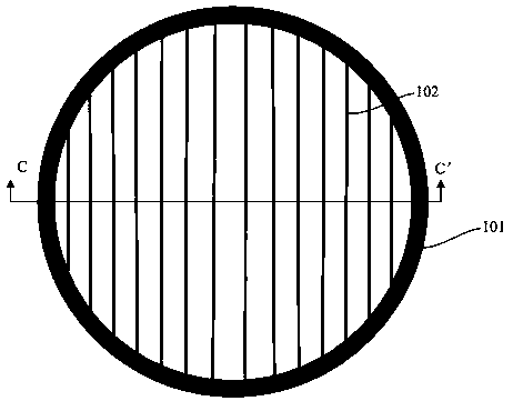
[0068] Such as Figure 10~Figure 11 As shown, among them, Figure 11 shown as Figure 10 The schematic diagram of the cross-sectional structure at CC' in the middle, this embodiment provides a metal grid high-power vertical cavity surface emitting laser, its basic structure is as in embodiment 1, wherein, the difference from embodiment 1 is that the The plurality of grid line electrodes 102 of the upper electrode are connected to the peripheral electrode 101 at intervals, and are arranged in parallel in the emission hole 100. The polarization structure is formed by the plurality of grid line electrodes 102. By adjusting multiple The distance between the grid wire electrodes 102 is used to adjust the polarization degree of the outgoing light of the vertical cavity surface emitting laser. For example, the smaller the distance between the multiple grid wire electrodes 102, the more the vertical cavity surface emitting laser The higher the degree of polarization of the laser lig...
PUM
 Abstract
Description
Claims
Application Information


